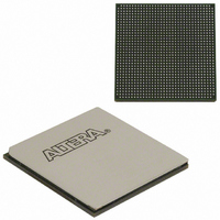
EP1AGX90EF1152I6N Altera, EP1AGX90EF1152I6N Datasheet - Page 116

EP1AGX90EF1152I6N
Manufacturer Part Number
EP1AGX90EF1152I6N
Description
IC ARRIA GX FPGA 90K 1152FBGA
Manufacturer
Altera
Series
Arria GXr
Datasheet
1.EP1AGX20CF484C6N.pdf
(234 pages)
Specifications of EP1AGX90EF1152I6N
Number Of Logic Elements/cells
90220
Number Of Labs/clbs
4511
Total Ram Bits
4477824
Number Of I /o
538
Voltage - Supply
1.15 V ~ 1.25 V
Mounting Type
Surface Mount
Operating Temperature
-40°C ~ 100°C
Package / Case
1152-FBGA
Lead Free Status / RoHS Status
Lead free / RoHS Compliant
Number Of Gates
-
Other names
544-2387
Available stocks
Company
Part Number
Manufacturer
Quantity
Price
- Current page: 116 of 234
- Download datasheet (4Mb)
3–4
Operating Modes
Arria GX Device Handbook, Volume 1
In addition to the number of configuration methods supported, Arria GX devices also
offer decompression and remote system upgrade features. The decompression feature
allows Arria GX FPGAs to receive a compressed configuration bitstream and
decompress this data in real-time, reducing storage requirements and configuration
time. The remote system upgrade feature allows real-time system upgrades from
remote locations of Arria GX designs. For more information, refer to
Schemes” on page
The Arria GX architecture uses SRAM configuration elements that require
configuration data to be loaded each time the circuit powers up. The process of
physically loading the SRAM data into the device is called configuration. During
initialization, which occurs immediately after configuration, the device resets
registers, enables I/O pins, and begins to operate as a logic device. The I/O pins are
tri-stated during power up, and before and during configuration. Together, the
configuration and initialization processes are called command mode. Normal device
operation is called user mode.
SRAM configuration elements allow you to reconfigure Arria GX devices in-circuit by
loading new configuration data into the device. With real-time reconfiguration, the
device is forced into command mode with a device pin. The configuration process
loads different configuration data, re-initializes the device, and resumes user-mode
operation. You can perform in-field upgrades by distributing new configuration files
either within the system or remotely.
PORSEL is a dedicated input pin used to select power-on reset (POR) delay times of
12 ms or 100 ms during power up. When the PORSEL pin is connected to ground, the
POR time is 100 ms. When the PORSEL pin is connected to V
The nIO_PULLUP pin is a dedicated input that chooses whether the internal pull-up
resistors on the user I/O pins and dual-purpose configuration I/O pins (nCSO, ASDO,
DATA[7..0], nWS, nRS, RDYnBSY, nCS, CS, RUnLU, PGM[2..0], CLKUSR,
INIT_DONE, DEV_OE, DEV_CLR) are on or off before and during configuration. A
logic high (1.5, 1.8, 2.5, 3.3 V) turns off the weak internal pull-up resistors, while a
logic low turns them on.
Arria GX devices also offer a new power supply, V
3.3 V in order to power the 3.3-V/2.5-V buffer available on the configuration input
pins and JTAG pins. V
TRST) and the following configuration pins: nCONFIG, DCLK (when used as an input),
nIO_PULLUP, DATA[7..0], RUnLU, nCE, nWS, nRS, CS, nCS, and CLKUSR. The V
pin allows the V
independent of the voltage required by the configuration inputs. Therefore, when
selecting the V
the configuration inputs into consideration. The configuration input pins, nCONFIG,
DCLK (when used as an input), nIO_PULLUP, RUnLU, nCE, nWS, nRS, CS, nCS, and
CLKUSR, have a dual buffer design: a 3.3-V/2.5-V input buffer and a 1.8-V/1.5-V
input buffer. The V
input buffer is powered by V
V
CCIO
.
CCIO
CCIO
3–5.
voltage, you do not have to take the VIL and VIH levels driven to
CCSEL
setting (of the banks where the configuration inputs reside) to be
CCPD
input pin selects which input buffer is used. The 3.3-V/2.5-V
applies to all the JTAG input pins (TCK, TMS, TDI, and
CCPD
, while the 1.8-V/1.5-V input buffer is powered by
C CPD
, which must be connected to
© December 2009 Altera Corporation
Chapter 3: Configuration and Testing
CC
, the POR time is 12 ms.
“Configuration
Configuration
CCSEL
Related parts for EP1AGX90EF1152I6N
Image
Part Number
Description
Manufacturer
Datasheet
Request
R

Part Number:
Description:
CYCLONE II STARTER KIT EP2C20N
Manufacturer:
Altera
Datasheet:

Part Number:
Description:
CPLD, EP610 Family, ECMOS Process, 300 Gates, 16 Macro Cells, 16 Reg., 16 User I/Os, 5V Supply, 35 Speed Grade, 24DIP
Manufacturer:
Altera Corporation
Datasheet:

Part Number:
Description:
CPLD, EP610 Family, ECMOS Process, 300 Gates, 16 Macro Cells, 16 Reg., 16 User I/Os, 5V Supply, 15 Speed Grade, 24DIP
Manufacturer:
Altera Corporation
Datasheet:

Part Number:
Description:
Manufacturer:
Altera Corporation
Datasheet:

Part Number:
Description:
CPLD, EP610 Family, ECMOS Process, 300 Gates, 16 Macro Cells, 16 Reg., 16 User I/Os, 5V Supply, 30 Speed Grade, 24DIP
Manufacturer:
Altera Corporation
Datasheet:

Part Number:
Description:
High-performance, low-power erasable programmable logic devices with 8 macrocells, 10ns
Manufacturer:
Altera Corporation
Datasheet:

Part Number:
Description:
High-performance, low-power erasable programmable logic devices with 8 macrocells, 7ns
Manufacturer:
Altera Corporation
Datasheet:

Part Number:
Description:
Classic EPLD
Manufacturer:
Altera Corporation
Datasheet:

Part Number:
Description:
High-performance, low-power erasable programmable logic devices with 8 macrocells, 10ns
Manufacturer:
Altera Corporation
Datasheet:

Part Number:
Description:
Manufacturer:
Altera Corporation
Datasheet:

Part Number:
Description:
Manufacturer:
Altera Corporation
Datasheet:

Part Number:
Description:
Manufacturer:
Altera Corporation
Datasheet:

Part Number:
Description:
CPLD, EP610 Family, ECMOS Process, 300 Gates, 16 Macro Cells, 16 Reg., 16 User I/Os, 5V Supply, 25 Speed Grade, 24DIP
Manufacturer:
Altera Corporation
Datasheet:


