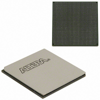
EP1AGX90EF1152I6N Altera, EP1AGX90EF1152I6N Datasheet - Page 70

EP1AGX90EF1152I6N
Manufacturer Part Number
EP1AGX90EF1152I6N
Description
IC ARRIA GX FPGA 90K 1152FBGA
Manufacturer
Altera
Series
Arria GXr
Datasheet
1.EP1AGX20CF484C6N.pdf
(234 pages)
Specifications of EP1AGX90EF1152I6N
Number Of Logic Elements/cells
90220
Number Of Labs/clbs
4511
Total Ram Bits
4477824
Number Of I /o
538
Voltage - Supply
1.15 V ~ 1.25 V
Mounting Type
Surface Mount
Operating Temperature
-40°C ~ 100°C
Package / Case
1152-FBGA
Lead Free Status / RoHS Status
Lead free / RoHS Compliant
Number Of Gates
-
Other names
544-2387
Available stocks
Company
Part Number
Manufacturer
Quantity
Price
- Current page: 70 of 234
- Download datasheet (4Mb)
2–64
Figure 2–53. DSP Block Interface to Interconnect
Arria GX Device Handbook, Volume 1
f
C4 Interconnect
LAB
A bus of 44 control signals feeds the entire DSP block. These signals include clocks,
asynchronous clears, clock enables, signed and unsigned control signals, addition and
subtraction control signals, rounding and saturation control signals, and accumulator
synchronous loads. The clock signals are routed from LAB row clocks and are
generated from specific LAB rows at the DSP block interface. The LAB row source for
control signals, data inputs, and outputs is shown in
For more information about DSP blocks, refer to the
chapter.
18
DSP Block to
LAB Row Interface
Block Interconnect Region
Direct Link Interconnect
from Adjacent LAB
36
16
Row Interface
36
12
Block
36 Inputs per Row
R4 Interconnect
16
Control
A[17..0]
B[17..0]
DSP Block
Row Structure
OA[17..0]
OB[17..0]
36 Outputs per Row
Direct Link Outputs
to Adjacent LABs
36
DSP Blocks in Arria GX Devices
36
Table
© December 2009 Altera Corporation
2–15.
Chapter 2: Arria GX Architecture
Direct Link Interconnect
from Adjacent LAB
Digital Signal Processing Block
LAB
Related parts for EP1AGX90EF1152I6N
Image
Part Number
Description
Manufacturer
Datasheet
Request
R

Part Number:
Description:
CYCLONE II STARTER KIT EP2C20N
Manufacturer:
Altera
Datasheet:

Part Number:
Description:
CPLD, EP610 Family, ECMOS Process, 300 Gates, 16 Macro Cells, 16 Reg., 16 User I/Os, 5V Supply, 35 Speed Grade, 24DIP
Manufacturer:
Altera Corporation
Datasheet:

Part Number:
Description:
CPLD, EP610 Family, ECMOS Process, 300 Gates, 16 Macro Cells, 16 Reg., 16 User I/Os, 5V Supply, 15 Speed Grade, 24DIP
Manufacturer:
Altera Corporation
Datasheet:

Part Number:
Description:
Manufacturer:
Altera Corporation
Datasheet:

Part Number:
Description:
CPLD, EP610 Family, ECMOS Process, 300 Gates, 16 Macro Cells, 16 Reg., 16 User I/Os, 5V Supply, 30 Speed Grade, 24DIP
Manufacturer:
Altera Corporation
Datasheet:

Part Number:
Description:
High-performance, low-power erasable programmable logic devices with 8 macrocells, 10ns
Manufacturer:
Altera Corporation
Datasheet:

Part Number:
Description:
High-performance, low-power erasable programmable logic devices with 8 macrocells, 7ns
Manufacturer:
Altera Corporation
Datasheet:

Part Number:
Description:
Classic EPLD
Manufacturer:
Altera Corporation
Datasheet:

Part Number:
Description:
High-performance, low-power erasable programmable logic devices with 8 macrocells, 10ns
Manufacturer:
Altera Corporation
Datasheet:

Part Number:
Description:
Manufacturer:
Altera Corporation
Datasheet:

Part Number:
Description:
Manufacturer:
Altera Corporation
Datasheet:

Part Number:
Description:
Manufacturer:
Altera Corporation
Datasheet:

Part Number:
Description:
CPLD, EP610 Family, ECMOS Process, 300 Gates, 16 Macro Cells, 16 Reg., 16 User I/Os, 5V Supply, 25 Speed Grade, 24DIP
Manufacturer:
Altera Corporation
Datasheet:


