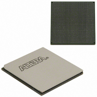
EP1AGX90EF1152I6N Altera, EP1AGX90EF1152I6N Datasheet - Page 128

EP1AGX90EF1152I6N
Manufacturer Part Number
EP1AGX90EF1152I6N
Description
IC ARRIA GX FPGA 90K 1152FBGA
Manufacturer
Altera
Series
Arria GXr
Datasheet
1.EP1AGX20CF484C6N.pdf
(234 pages)
Specifications of EP1AGX90EF1152I6N
Number Of Logic Elements/cells
90220
Number Of Labs/clbs
4511
Total Ram Bits
4477824
Number Of I /o
538
Voltage - Supply
1.15 V ~ 1.25 V
Mounting Type
Surface Mount
Operating Temperature
-40°C ~ 100°C
Package / Case
1152-FBGA
Lead Free Status / RoHS Status
Lead free / RoHS Compliant
Number Of Gates
-
Other names
544-2387
Available stocks
Company
Part Number
Manufacturer
Quantity
Price
- Current page: 128 of 234
- Download datasheet (4Mb)
4–6
Table 4–6. Arria GX Transceiver Block AC Specification (Part 3 of 3)
Arria GX Device Handbook, Volume 1
Transmitter PLL
VCO frequency range
Bandwidth at 3.125 Gbps
Bandwidth at 2.5 Gbps
TX PLL lock time from gxb_powerdown
de-assertion (9),
PCS
Interface speed per mode
Digital Reset Pulse Width
Notes to
(1) Spread spectrum clocking is allowed only in PCI Express (PIPE) mode if the upstream transmitter and the receiver share the same clock source.
(2) The reference clock DC coupling option is only available in PCI Express (PIPE) mode for the HCSL I/O standard.
(3) The fixedclk is used in PIPE mode receiver detect circuitry.
(4) The device cannot tolerate prolonged operation at this absolute maximum.
(5) The rate matcher supports only up to ± 300 PPM for PIPE mode and ± 100 PPM for GIGE mode.
(6) This parameter is measured by embedding the run length data in a PRBS sequence.
(7) Signal detect threshold detector circuitry is available only in PCI Express (PIPE mode).
(8) Time taken for rx_pll_locked to go high from rx_analogreset deassertion. Refer to
(9) For lock times specific to the protocols, refer to protocol characterization documents.
(10) Time for which the CDR needs to stay in LTR mode after rx_pll_locked is asserted and before rx_locktodata is asserted in manual
(11) Time taken to recover valid data from GXB after the rx_locktodata signal is asserted in manual mode. Measurement results are based on
(12) Time taken to recover valid data from GXB after the rx_freqlocked signal goes high in automatic mode. Measurement results are based
(13) This is applicable only to PCI Express (PIPE) ×4 and XAUI ×4 mode.
(14) Time taken to lock TX PLL from gxb_powerdown deassertion.
(15) The 1.2 V RX VICM settings is intended for DC-coupled LVDS links.
mode. Refer to
PRBS31, for native data rates only. Refer to
on PRBS31, for native data rates only. Refer to
Table
Symbol / Description
4–6:
1
(14)
Figure
Figure 4–1
lock time parameters in automatic mode.
LTD = Lock to data
LTR = Lock to reference clock
4–1.
shows the lock time parameters in manual mode.
Figure
Figure
4–1.
4–2.
Conditions
BW = High
BW = High
BW = Low
BW = Med
BW = Low
BW = Med
—
—
—
—
Minimum is 2 parallel clock cycles
–6 Speed Grade Commercial and
Min
500
—
—
—
—
—
—
—
25
Industrial
Figure
Chapter 4: DC and Switching Characteristics
Typ
—
—
—
3
5
9
1
2
4
4–1.
© December 2009 Altera Corporation
Figure 4–2
1562.5
156.25
Max
100
—
—
—
—
—
—
Operating Conditions
shows the
Units
MHz
MHz
MHz
MHz
us
—
Related parts for EP1AGX90EF1152I6N
Image
Part Number
Description
Manufacturer
Datasheet
Request
R

Part Number:
Description:
CYCLONE II STARTER KIT EP2C20N
Manufacturer:
Altera
Datasheet:

Part Number:
Description:
CPLD, EP610 Family, ECMOS Process, 300 Gates, 16 Macro Cells, 16 Reg., 16 User I/Os, 5V Supply, 35 Speed Grade, 24DIP
Manufacturer:
Altera Corporation
Datasheet:

Part Number:
Description:
CPLD, EP610 Family, ECMOS Process, 300 Gates, 16 Macro Cells, 16 Reg., 16 User I/Os, 5V Supply, 15 Speed Grade, 24DIP
Manufacturer:
Altera Corporation
Datasheet:

Part Number:
Description:
Manufacturer:
Altera Corporation
Datasheet:

Part Number:
Description:
CPLD, EP610 Family, ECMOS Process, 300 Gates, 16 Macro Cells, 16 Reg., 16 User I/Os, 5V Supply, 30 Speed Grade, 24DIP
Manufacturer:
Altera Corporation
Datasheet:

Part Number:
Description:
High-performance, low-power erasable programmable logic devices with 8 macrocells, 10ns
Manufacturer:
Altera Corporation
Datasheet:

Part Number:
Description:
High-performance, low-power erasable programmable logic devices with 8 macrocells, 7ns
Manufacturer:
Altera Corporation
Datasheet:

Part Number:
Description:
Classic EPLD
Manufacturer:
Altera Corporation
Datasheet:

Part Number:
Description:
High-performance, low-power erasable programmable logic devices with 8 macrocells, 10ns
Manufacturer:
Altera Corporation
Datasheet:

Part Number:
Description:
Manufacturer:
Altera Corporation
Datasheet:

Part Number:
Description:
Manufacturer:
Altera Corporation
Datasheet:

Part Number:
Description:
Manufacturer:
Altera Corporation
Datasheet:

Part Number:
Description:
CPLD, EP610 Family, ECMOS Process, 300 Gates, 16 Macro Cells, 16 Reg., 16 User I/Os, 5V Supply, 25 Speed Grade, 24DIP
Manufacturer:
Altera Corporation
Datasheet:


