EP2S130F1508C4N Altera, EP2S130F1508C4N Datasheet - Page 215
EP2S130F1508C4N
Manufacturer Part Number
EP2S130F1508C4N
Description
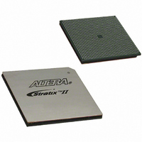
IC STRATIX II FPGA 130K 1508FBGA
Manufacturer
Altera
Series
Stratix® IIr
Datasheet
1.EP2S15F484I4N.pdf
(238 pages)
Specifications of EP2S130F1508C4N
Number Of Logic Elements/cells
132540
Number Of Labs/clbs
6627
Total Ram Bits
6747840
Number Of I /o
1126
Voltage - Supply
1.15 V ~ 1.25 V
Mounting Type
Surface Mount
Operating Temperature
0°C ~ 85°C
Package / Case
1508-FBGA
Lead Free Status / RoHS Status
Lead free / RoHS Compliant
Number Of Gates
-
Other names
544-1870
EP2S130F1508C4N
EP2S130F1508C4N
Available stocks
Company
Part Number
Manufacturer
Quantity
Price
Company:

Part Number:
EP2S130F1508C4N
Manufacturer:
ALTERA
Quantity:
490
Part Number:
EP2S130F1508C4N
Manufacturer:
ALTERA/阿尔特拉
Quantity:
20 000


Figure 5–9. DCD Measurement Technique for DDIO (Double-Data Rate) Outputs
Altera Corporation
April 2011
clk
INPUT
VCC
However, when the output is a double data rate input/output (DDIO)
signal, both edges of the input clock signal (positive and negative) trigger
output transitions
clock and the input clock buffer affect the output DCD.
When an FPGA PLL generates the internal clock, the PLL output clocks
the IOE block. As the PLL only monitors the positive edge of the reference
clock input and internally re-creates the output clock signal, any DCD
present on the reference clock is filtered out. Therefore, the DCD for a
DDIO output with PLL in the clock path is better than the DCD for a
DDIO output without PLL in the clock path.
Tables 5–80
derivation for different I/O standards on Stratix II devices. Examples are
also provided that show how to calculate DCD as a percentage.
IOE
3.3-V LVTTTL
3.3-V LVCMOS
2.5 V
Table 5–80. Maximum DCD for Non-DDIO Output on Row I/O Pins (Part 1
of 2)
Row I/O Output
Standard
NOT
inst8
Note (1)
through
GND
V
CC
(Figure
DFF
inst2
DFF
inst3
5–87
D
D
CLRN
CLRN
PRN
PRN
-3 Devices
give the maximum DCD in absolution
5–9). Therefore, any distortion on the input
Q
Q
245
125
105
Maximum DCD for Non-DDIO Output
Stratix II Device Handbook, Volume 1
-4 & -5 Devices
DC & Switching Characteristics
275
155
135
OUTPUT
output
Unit
ps
ps
ps
5–79
Related parts for EP2S130F1508C4N
Image
Part Number
Description
Manufacturer
Datasheet
Request
R

Part Number:
Description:
CYCLONE II STARTER KIT EP2C20N
Manufacturer:
Altera
Datasheet:


Part Number:
Description:
CPLD, EP610 Family, ECMOS Process, 300 Gates, 16 Macro Cells, 16 Reg., 16 User I/Os, 5V Supply, 35 Speed Grade, 24DIP
Manufacturer:
Altera Corporation
Datasheet:
Part Number:
Description:
CPLD, EP610 Family, ECMOS Process, 300 Gates, 16 Macro Cells, 16 Reg., 16 User I/Os, 5V Supply, 15 Speed Grade, 24DIP
Manufacturer:
Altera Corporation
Datasheet:
Part Number:
Description:
Manufacturer:
Altera Corporation
Datasheet:
Part Number:
Description:
CPLD, EP610 Family, ECMOS Process, 300 Gates, 16 Macro Cells, 16 Reg., 16 User I/Os, 5V Supply, 30 Speed Grade, 24DIP
Manufacturer:
Altera Corporation
Datasheet:
Part Number:
Description:
High-performance, low-power erasable programmable logic devices with 8 macrocells, 10ns
Manufacturer:
Altera Corporation
Datasheet:
Part Number:
Description:
High-performance, low-power erasable programmable logic devices with 8 macrocells, 7ns
Manufacturer:
Altera Corporation
Datasheet:
Part Number:
Description:
Classic EPLD
Manufacturer:
Altera Corporation
Datasheet:
Part Number:
Description:
High-performance, low-power erasable programmable logic devices with 8 macrocells, 10ns
Manufacturer:
Altera Corporation
Datasheet:
Part Number:
Description:
Manufacturer:
Altera Corporation
Datasheet:
Part Number:
Description:
Manufacturer:
Altera Corporation
Datasheet:
Part Number:
Description:
Manufacturer:
Altera Corporation
Datasheet:
Part Number:
Description:
CPLD, EP610 Family, ECMOS Process, 300 Gates, 16 Macro Cells, 16 Reg., 16 User I/Os, 5V Supply, 25 Speed Grade, 24DIP
Manufacturer:
Altera Corporation
Datasheet: