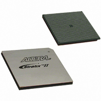
EP2S130F1508C4N Altera, EP2S130F1508C4N Datasheet - Page 76

EP2S130F1508C4N
Manufacturer Part Number
EP2S130F1508C4N
Description
IC STRATIX II FPGA 130K 1508FBGA
Manufacturer
Altera
Series
Stratix® IIr
Datasheet
1.EP2S15F484I4N.pdf
(238 pages)
Specifications of EP2S130F1508C4N
Number Of Logic Elements/cells
132540
Number Of Labs/clbs
6627
Total Ram Bits
6747840
Number Of I /o
1126
Voltage - Supply
1.15 V ~ 1.25 V
Mounting Type
Surface Mount
Operating Temperature
0°C ~ 85°C
Package / Case
1508-FBGA
Lead Free Status / RoHS Status
Lead free / RoHS Compliant
Number Of Gates
-
Other names
544-1870
EP2S130F1508C4N
EP2S130F1508C4N
Available stocks
Company
Part Number
Manufacturer
Quantity
Price
Company:
Part Number:
EP2S130F1508C4N
Manufacturer:
ALTERA
Quantity:
490
Part Number:
EP2S130F1508C4N
Manufacturer:
ALTERA/阿尔特拉
Quantity:
20 000
- Current page: 76 of 238
- Download datasheet (3Mb)
PLLs & Clock Networks
Figure 2–44. Stratix II Enhanced PLL
Notes to
(1)
(2)
(3)
(4)
2–68
Stratix II Device Handbook, Volume 1
Global or
Regional
Clock
INCLK[3..0]
Each clock source can come from any of the four clock pins that are physically located on the same side of the device
as the PLL.
If the feedback input is used, you lose one (or two, if FBIN is differential) external clock output pin.
Each enhanced PLL has three differential external clock outputs or six single-ended external clock outputs.
The global or regional clock input can be driven by an output from another PLL, a pin-driven dedicated global or
regional clock, or through a clock control block, provided the clock control block is fed by an output from another
PLL or a pin-driven dedicated global or regional clock. An internally generated global signal cannot drive the PLL.
(4)
Figure
4
Shaded Portions of the
PLL are Reconfigurable
2–44:
FBIN
Switchover
Circuitry
Clock
(2)
Enhanced PLLs
Stratix II devices contain up to four enhanced PLLs with advanced clock
management features.
/n
Phase Frequency
Detector
PFD
Note (1)
Charge
Pump
Lock Detect
& Filter
Spectrum
Spread
/m
Filter
Loop
VCO Phase Selection
Affecting All Outputs
VCO Phase Selection
Selectable at Each
PLL Output Port
Figure 2–44
VCO
8
shows a diagram of the enhanced PLL.
Post-Scale
Counters
/c0
/c1
/c2
/c3
/c4
/c5
From Adjacent PLL
6
Altera Corporation
4
8
6
Global
Clocks
Regional
Clocks
I/O Buffers (3)
to I/O or general
routing
May 2007
Related parts for EP2S130F1508C4N
Image
Part Number
Description
Manufacturer
Datasheet
Request
R

Part Number:
Description:
CYCLONE II STARTER KIT EP2C20N
Manufacturer:
Altera
Datasheet:

Part Number:
Description:
CPLD, EP610 Family, ECMOS Process, 300 Gates, 16 Macro Cells, 16 Reg., 16 User I/Os, 5V Supply, 35 Speed Grade, 24DIP
Manufacturer:
Altera Corporation
Datasheet:

Part Number:
Description:
CPLD, EP610 Family, ECMOS Process, 300 Gates, 16 Macro Cells, 16 Reg., 16 User I/Os, 5V Supply, 15 Speed Grade, 24DIP
Manufacturer:
Altera Corporation
Datasheet:

Part Number:
Description:
Manufacturer:
Altera Corporation
Datasheet:

Part Number:
Description:
CPLD, EP610 Family, ECMOS Process, 300 Gates, 16 Macro Cells, 16 Reg., 16 User I/Os, 5V Supply, 30 Speed Grade, 24DIP
Manufacturer:
Altera Corporation
Datasheet:

Part Number:
Description:
High-performance, low-power erasable programmable logic devices with 8 macrocells, 10ns
Manufacturer:
Altera Corporation
Datasheet:

Part Number:
Description:
High-performance, low-power erasable programmable logic devices with 8 macrocells, 7ns
Manufacturer:
Altera Corporation
Datasheet:

Part Number:
Description:
Classic EPLD
Manufacturer:
Altera Corporation
Datasheet:

Part Number:
Description:
High-performance, low-power erasable programmable logic devices with 8 macrocells, 10ns
Manufacturer:
Altera Corporation
Datasheet:

Part Number:
Description:
Manufacturer:
Altera Corporation
Datasheet:

Part Number:
Description:
Manufacturer:
Altera Corporation
Datasheet:

Part Number:
Description:
Manufacturer:
Altera Corporation
Datasheet:

Part Number:
Description:
CPLD, EP610 Family, ECMOS Process, 300 Gates, 16 Macro Cells, 16 Reg., 16 User I/Os, 5V Supply, 25 Speed Grade, 24DIP
Manufacturer:
Altera Corporation
Datasheet:


