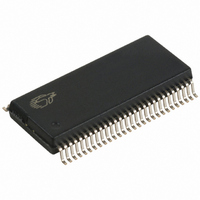
CY7C68013-56PVXC Cypress Semiconductor Corp, CY7C68013-56PVXC Datasheet - Page 28

CY7C68013-56PVXC
Manufacturer Part Number
CY7C68013-56PVXC
Description
IC MCU USB PERIPH HI SPD 56SSOP
Manufacturer
Cypress Semiconductor Corp
Series
EZ-USB FX2LP™r
Datasheet
1.CY7C68013-56PVC.pdf
(52 pages)
Specifications of CY7C68013-56PVXC
Applications
USB Microcontroller
Core Processor
8051
Program Memory Type
ROMless
Controller Series
CY7C680xx
Ram Size
16K x 8
Interface
I²C, USB, USART
Number Of I /o
24
Voltage - Supply
3 V ~ 3.6 V
Operating Temperature
0°C ~ 70°C
Mounting Type
Surface Mount
Package / Case
56-SSOP
Lead Free Status / RoHS Status
Lead free / RoHS Compliant
Other names
428-1623
Available stocks
Company
Part Number
Manufacturer
Quantity
Price
Company:
Part Number:
CY7C68013-56PVXC
Manufacturer:
CY
Quantity:
5 530
Company:
Part Number:
CY7C68013-56PVXC
Manufacturer:
CY
Quantity:
6 100
Company:
Part Number:
CY7C68013-56PVXC
Manufacturer:
SAM
Quantity:
2 000
Part Number:
CY7C68013-56PVXC
Manufacturer:
CYPRESS/赛普拉斯
Quantity:
20 000
Table 4-1. FX2 Pin Descriptions (continued)
Document #: 38-08012 Rev. *C
TQFP
128
110
111
112
113
114
115
4
5
6
7
8
9
TQFP
100
88
89
90
91
92
93
3
4
5
6
7
8
SSOP
56
8
9
QFN
56
1
2
PE2 or
T2OUT
PE3 or
RXD0OUT
PE4 or
RXD1OUT
PE5 or
INT6
PE6 or
T2EX
PE7 or
GPIFADR8
RDY0 or
SLRD
RDY1 or
SLWR
RDY2
RDY3
RDY4
RDY5
Name
Type
I/O/Z
I/O/Z
I/O/Z
I/O/Z
I/O/Z
I/O/Z
Input
Input
Input
Input
Input
Input
[5]
Default
(PE2)
(PE3)
(PE4)
(PE5)
(PE6)
(PE7)
N/A
N/A
N/A
N/A
N/A
N/A
I
I
I
I
I
I
Multiplexed pin whose function is selected by the PORTECFG.2
bit.
PE2 is a bidirectional I/O port pin.
T2OUT is the active-HIGH output signal from 8051 Timer2.
T2OUT is active (HIGH) for one clock cycle when Timer/Counter
2 overflows.
Multiplexed pin whose function is selected by the PORTECFG.3
bit.
PE3 is a bidirectional I/O port pin.
RXD0OUT is an active-HIGH signal from 8051 UART0. If
RXD0OUT is selected and UART0 is in Mode 0, this pin provides
the output data for UART0 only when it is in sync mode. Otherwise
it is a 1.
Multiplexed pin whose function is selected by the PORTECFG.4
bit.
PE4 is a bidirectional I/O port pin.
RXD1OUT is an active-HIGH output from 8051 UART1. When
RXD1OUT is selected and UART1 is in Mode 0, this pin provides
the output data for UART1 only when it is in sync mode. In Modes
1, 2, and 3, this pin is HIGH.
Multiplexed pin whose function is selected by the PORTECFG.5
bit.
PE5 is a bidirectional I/O port pin.
INT6 is the 8051 INT5 interrupt request input signal. The INT6 pin
is edge-sensitive, active HIGH.
Multiplexed pin whose function is selected by the PORTECFG.6
bit.
PE6 is a bidirectional I/O port pin.
T2EX is an active-high input signal to the 8051 Timer2. T2EX
reloads timer 2 on its falling edge. T2EX is active only if the EXEN2
bit is set in T2CON.
Multiplexed pin whose function is selected by the PORTECFG.7
bit.
PE7 is a bidirectional I/O port pin.
GPIFADR8 is a GPIF address output pin.
Multiplexed pin whose function is selected by the following bits:
IFCONFIG[1..0].
RDY0 is a GPIF input signal.
SLRD is the input-only read strobe with programmable polarity
(FIFOPOLAR.3) for the slave FIFOs connected to FDI[7..0] or
FDI[15..0].
Multiplexed pin whose function is selected by the following bits:
IFCONFIG[1..0].
RDY1 is a GPIF input signal.
SLWR is the input-only write strobe with programmable polarity
(FIFOPOLAR.2) for the slave FIFOs connected to FDI[7..0] or
FDI[15..0].
RDY2 is a GPIF input signal.
RDY3 is a GPIF input signal.
RDY4 is a GPIF input signal.
RDY5 is a GPIF input signal.
Description
CY7C68013
Page 28 of 52


