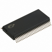
CY7C68013-56PVXC Cypress Semiconductor Corp, CY7C68013-56PVXC Datasheet - Page 29

CY7C68013-56PVXC
Manufacturer Part Number
CY7C68013-56PVXC
Description
IC MCU USB PERIPH HI SPD 56SSOP
Manufacturer
Cypress Semiconductor Corp
Series
EZ-USB FX2LP™r
Datasheet
1.CY7C68013-56PVC.pdf
(52 pages)
Specifications of CY7C68013-56PVXC
Applications
USB Microcontroller
Core Processor
8051
Program Memory Type
ROMless
Controller Series
CY7C680xx
Ram Size
16K x 8
Interface
I²C, USB, USART
Number Of I /o
24
Voltage - Supply
3 V ~ 3.6 V
Operating Temperature
0°C ~ 70°C
Mounting Type
Surface Mount
Package / Case
56-SSOP
Lead Free Status / RoHS Status
Lead free / RoHS Compliant
Other names
428-1623
Available stocks
Company
Part Number
Manufacturer
Quantity
Price
Company:
Part Number:
CY7C68013-56PVXC
Manufacturer:
CY
Quantity:
5 530
Company:
Part Number:
CY7C68013-56PVXC
Manufacturer:
CY
Quantity:
6 100
Company:
Part Number:
CY7C68013-56PVXC
Manufacturer:
SAM
Quantity:
2 000
Part Number:
CY7C68013-56PVXC
Manufacturer:
CYPRESS/赛普拉斯
Quantity:
20 000
Table 4-1. FX2 Pin Descriptions (continued)
Document #: 38-08012 Rev. *C
TQFP
128
106
69
70
71
66
67
98
32
28
31
30
29
53
52
51
50
42
41
TQFP
100
54
55
56
51
52
76
26
22
84
25
24
23
43
42
41
40
32
SSOP
56
36
37
38
20
QFN
56
29 CTL0 or
30 CTL1 or
31 CTL2 or
13 IFCLK
FLAGA
FLAGB
FLAGC
CTL3
CTL4
CTL5
INT4
INT5#
T2
T1
T0
RXD1
TXD1
RXD0
TXD0
CS#
WR#
Name
Output
Output
Output
Output
Output
Output
Output
Output
Output
Output
Type
I/O/Z
Input
Input
Input
Input
Input
Input
Input
[5]
Default
N/A
N/A
N/A
N/A
N/A
N/A
N/A
H
H
H
H
H
H
H
H
H
H
Z
Multiplexed pin whose function is selected by the following bits:
IFCONFIG[1..0].
CTL0 is a GPIF control output.
FLAGA is a programmable slave-FIFO output status flag signal.
Defaults to programmable for the FIFO selected by the
FIFOADR[1:0] pins.
Multiplexed pin whose function is selected by the following bits:
IFCONFIG[1..0].
CTL1 is a GPIF control output.
FLAGB is a programmable slave-FIFO output status flag signal.
Defaults to FULL for the FIFO selected by the FIFOADR[1:0] pins.
Multiplexed pin whose function is selected by the following bits:
IFCONFIG[1..0].
CTL2 is a GPIF control output.
FLAGC is a programmable slave-FIFO output status flag signal.
Defaults to EMPTY for the FIFO selected by the FIFOADR[1:0]
pins.
CTL3 is a GPIF control output.
CTL4 is a GPIF control output.
CTL5 is a GPIF control output.
Interface Clock, used for synchronously clocking data into or out
of the slave FIFOs. IFCLK also serves as a timing reference for all
slave FIFO control signals and GPIF. When internal clocking,
IFCONFIG.7 = 1, is used the IFCLK pin can be configured to
output 30/48 MHz by bits IFCONFIG.5 and IFCONFIG.6. IFCLK
may be inverted, whether internally or externally sourced, by
setting the bit
IFCONFIG.4 =1.
INT4 is the 8051 INT4 interrupt request input signal. The INT4 pin
is edge-sensitive, active HIGH.
INT5# is the 8051 INT5 interrupt request input signal. The INT5
pin is edge-sensitive, active LOW.
T2 is the active-HIGH T2 input signal to 8051 Timer2, which
provides the input to Timer2 when C/T2 = 1. When C/T2 = 0,
Timer2 does not use this pin.
T1 is the active-HIGH T1 signal for 8051 Timer1, which provides
the input to Timer1 when C/T1 is 1. When C/T1 is 0, Timer1 does
not use this bit.
T0 is the active-HIGH T0 signal for 8051 Timer0, which provides
the input to Timer0 when C/T0 is 1. When C/T0 is 0, Timer0 does
not use this bit.
RXD1is an active-HIGH input signal for 8051 UART1, which
provides data to the UART in all modes.
TXD1is an active-HIGH output pin from 8051 UART1, which
provides the output clock in sync mode, and the output data in
async mode.
RXD0 is the active-HIGH RXD0 input to 8051 UART0, which
provides data to the UART in all modes.
TXD0 is the active-HIGH TXD0 output from 8051 UART0, which
provides the output clock in sync mode, and the output data in
async mode.
CS# is the active-LOW chip select for external memory.
WR# is the active-LOW write strobe output for external memory.
Description
CY7C68013
Page 29 of 52


