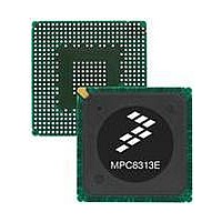
MPC8313CVRADDB Freescale Semiconductor, MPC8313CVRADDB Datasheet - Page 11

MPC8313CVRADDB
Manufacturer Part Number
MPC8313CVRADDB
Description
MPU POWERQUICC II PRO 516-PBGA
Manufacturer
Freescale Semiconductor
Datasheet
1.MPC8313CZQAFFB.pdf
(100 pages)
Specifications of MPC8313CVRADDB
Processor Type
MPC83xx PowerQUICC II Pro 32-Bit
Speed
267MHz
Voltage
0.95 V ~ 1.05 V
Mounting Type
Surface Mount
Package / Case
516-PBGA
Processor Series
MPC8xxx
Core
e300
Data Bus Width
32 bit
Development Tools By Supplier
MPC8313E-RDB
Maximum Clock Frequency
400 MHz
Operating Supply Voltage
- 0.3 V to + 1.26 V
Maximum Operating Temperature
+ 105 C
Mounting Style
SMD/SMT
Data Ram Size
16 KB
I/o Voltage
2.5 V
Interface Type
I2C, SPI, UART
Minimum Operating Temperature
- 40 C
Program Memory Type
EEPROM/Flash
Lead Free Status / RoHS Status
Lead free / RoHS Compliant
Features
-
Lead Free Status / Rohs Status
Lead free / RoHS Compliant
Available stocks
Company
Part Number
Manufacturer
Quantity
Price
Company:
Part Number:
MPC8313CVRADDB
Manufacturer:
FREESCAL
Quantity:
672
Company:
Part Number:
MPC8313CVRADDB
Manufacturer:
Freescale Semiconductor
Quantity:
10 000
Table 5
consume the amount of power described.
Table 6
D3 warm low-power state.
Freescale Semiconductor
DDR 1, 60% utilization,
50% read/write
R
R
single pair of clock
capacitive load: data = 8 pF,
control address = 8 pF,
clock = 8 pF
DDR 2, 60% utilization,
50% read/write
R
R
single pair of clock
capacitive load: data = 8 pF,
control address = 8 pF,
clock = 8 pF
PCI I/O load = 50 pF
Local bus I/O load = 20 pF
TSEC I/O load = 20 pF
USBDR controller load = 20 pF
Other I/O
1
s
t
s
t
= 50 Ω
= 75 Ω
= 22 Ω
= 22 Ω
describes a typical scenario where blocks with the stated percentage of utilization and impedances
shows the estimated core power dissipation of the MPC8313E while transitioning into the
Interface
1
2
3
MPC8313E PowerQUICC
All interfaces are enabled. For further power savings, disable the clocks to unused
blocks.
The interfaces are run at the following frequencies: DDR: 333 MHz, eLBC 83 MHz,
PCI 33 MHz, eTSEC1 and TSEC2: 167 MHz, SEC: 167 MHz, USB: 167 MHz. See
the SCCR register for more information.
This is maximum power in D3 Warm based on a voltage of 1.05 V and a junction
temperature of 105°C.
333-MHz Core, 167-MHz CSB
Table 6. MPC8313E Low-Power Modes Power Dissipation
Table 5. MPC8313E Typical I/O Power Dissipation
Parameter
333 MHz,
266 MHz,
333 MHz,
266 MHz,
125 MHz
D3 warm
33 MHz
66 MHz
66 MHz
50 MHz
25 MHz
60 MHz
RGMII,
32 bits
32 bits
32 bits
32 bits
MII,
—
(1.8 V)
GV
0.266
0.246
™
—
—
—
—
—
—
—
—
—
—
II Pro Processor Hardware Specifications, Rev. 3
DD
2
(2.5 V)
GV
0.355
0.323
—
—
—
—
—
—
—
—
—
—
DD
Rev. 1.0
400
(3.3 V)
NV
0.120
0.249
0.015
—
—
—
—
—
—
—
—
—
DD
3
LV
(3.3 V)
LV
0.008
0.078
0.078
—
—
—
—
—
—
—
—
—
DDA
DDB
Rev. 2.x or
/
Later
425
LV
(2.5 V)
LV
0.044
3
—
—
—
—
—
—
—
—
—
—
—
DDA
DDB
/
1
(3.3 V)
0.056
0.040
LV
Unit
mW
—
—
—
—
—
—
—
—
—
—
DD
Power Characteristics
Unit
W
W
W
W
W
W
W
W
W
W
W
W
Comments
Multiple by
number of
interface
used
—
—
—
—
—
—
—
—
—
—
11


