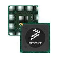
MPC8313CVRADDB Freescale Semiconductor, MPC8313CVRADDB Datasheet - Page 8

MPC8313CVRADDB
Manufacturer Part Number
MPC8313CVRADDB
Description
MPU POWERQUICC II PRO 516-PBGA
Manufacturer
Freescale Semiconductor
Datasheet
1.MPC8313CZQAFFB.pdf
(100 pages)
Specifications of MPC8313CVRADDB
Processor Type
MPC83xx PowerQUICC II Pro 32-Bit
Speed
267MHz
Voltage
0.95 V ~ 1.05 V
Mounting Type
Surface Mount
Package / Case
516-PBGA
Processor Series
MPC8xxx
Core
e300
Data Bus Width
32 bit
Development Tools By Supplier
MPC8313E-RDB
Maximum Clock Frequency
400 MHz
Operating Supply Voltage
- 0.3 V to + 1.26 V
Maximum Operating Temperature
+ 105 C
Mounting Style
SMD/SMT
Data Ram Size
16 KB
I/o Voltage
2.5 V
Interface Type
I2C, SPI, UART
Minimum Operating Temperature
- 40 C
Program Memory Type
EEPROM/Flash
Lead Free Status / RoHS Status
Lead free / RoHS Compliant
Features
-
Lead Free Status / Rohs Status
Lead free / RoHS Compliant
Available stocks
Company
Part Number
Manufacturer
Quantity
Price
Company:
Part Number:
MPC8313CVRADDB
Manufacturer:
FREESCAL
Quantity:
672
Company:
Part Number:
MPC8313CVRADDB
Manufacturer:
Freescale Semiconductor
Quantity:
10 000
Electrical Characteristics
amount of current listed in the Current Requirement column; this is the maximum current possible. Proper
device operation outside of these conditions is not guaranteed.
1
2
8
Core supply voltage
Internal core logic constant power
SerDes internal digital power
SerDes internal digital ground
SerDes I/O digital power
SerDes I/O digital ground
SerDes analog power for PLL
SerDes analog ground for PLL
Dedicated 3.3 V analog power for USB PLL
Dedicated 1.0 V analog power for USB PLL
Dedicated analog ground for USB PLL
Dedicated USB power for USB
Dedicated USB ground for USB bias circuit
Dedicated power for USB transceiver
Dedicated ground for USB transceiver
Analog power for e300 core APLL
Analog power for system APLL
DDR1 DRAM I/O voltage (333 MHz, 32-bit operation)
DDR2 DRAM I/O voltage (333 MHz, 32-bit operation)
Differential reference voltage for DDR controller
Standard I/O voltage
eTSEC2 IO supply
eTSEC1/USB DR IO supply
Supply for eLBC IOs
Analog and digital ground
Junction temperature
GV
direction.
Some GPIO pins may operate from a 2.5-V supply when configured for other functions.
DD
, NV
DD
, AV
DD
Characteristic
, and V
MPC8313E PowerQUICC
DD
bias
must track each other and must vary in the same direction—either in the positive or negative
Table 2. Recommended Operating Conditions
circuit
™
II Pro Processor Hardware Specifications, Rev. 3
USB_VDDA_BIAS
USB_VSSA_BIAS
USB_PLL_PWR3
USB_PLL_PWR1
USB_PLL_GND
XCOREV
USB_VDDA
XCOREV
USB_VSSA
XPADV
XPADV
SDAV
Symbol
SDAV
MV
AV
AV
LV
LV
GV
GV
NV
V
LV
V
V
DDC
T
DDB
DD
DDA
SS
DD1
DD2
REF
DD
DD
DD
DD
J
DD
SS
DD
SS
DD
SS
3.3 V ± 300 mV
2.5 V ± 125 mV/
2.5 V ± 125 mV/
Recommended
(0.49 × GV
3.3 V ± 300 mV
3.3 V ± 300 mV
3.3 V ± 300 mV
2.5 V ± 125 mV
1/2 DDR supply
3.3 V ± 300 mV
3.3 V ± 300 mV
3.3 V ± 300 mV
1.0 V ± 50 mV
1.0 V ± 50 mV
1.0 V ± 50 mV
1.0 V ± 50 mV
1.0 V ± 50 mV
1.0 V ± 50 mV
1.8 V ± 80 mV
0.51 × GV
0 to 105
Value
1.0
0.0
1.0
0.0
0.0
0.0
0.0
0.0
0.0
1
DD
DD
)
to
2
Freescale Semiconductor
Unit
°C
V
V
V
V
V
V
V
V
V
V
V
V
V
V
V
V
V
V
V
V
V
V
V
V
V
Requirement
Current
469 mA
377 mA
170 mA
2–3 mA
4–5 mA
2–3 mA
2–3 mA
131 mA
140 mA
2–3 mA
10 mA
10 mA
75 mA
74 mA
22 mA
44 mA
16 mA
—
—
—
—
—
—
—
—
—


