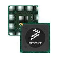
MPC8313CVRADDB Freescale Semiconductor, MPC8313CVRADDB Datasheet - Page 9

MPC8313CVRADDB
Manufacturer Part Number
MPC8313CVRADDB
Description
MPU POWERQUICC II PRO 516-PBGA
Manufacturer
Freescale Semiconductor
Datasheet
1.MPC8313CZQAFFB.pdf
(100 pages)
Specifications of MPC8313CVRADDB
Processor Type
MPC83xx PowerQUICC II Pro 32-Bit
Speed
267MHz
Voltage
0.95 V ~ 1.05 V
Mounting Type
Surface Mount
Package / Case
516-PBGA
Processor Series
MPC8xxx
Core
e300
Data Bus Width
32 bit
Development Tools By Supplier
MPC8313E-RDB
Maximum Clock Frequency
400 MHz
Operating Supply Voltage
- 0.3 V to + 1.26 V
Maximum Operating Temperature
+ 105 C
Mounting Style
SMD/SMT
Data Ram Size
16 KB
I/o Voltage
2.5 V
Interface Type
I2C, SPI, UART
Minimum Operating Temperature
- 40 C
Program Memory Type
EEPROM/Flash
Lead Free Status / RoHS Status
Lead free / RoHS Compliant
Features
-
Lead Free Status / Rohs Status
Lead free / RoHS Compliant
Available stocks
Company
Part Number
Manufacturer
Quantity
Price
Company:
Part Number:
MPC8313CVRADDB
Manufacturer:
FREESCAL
Quantity:
672
Company:
Part Number:
MPC8313CVRADDB
Manufacturer:
Freescale Semiconductor
Quantity:
10 000
Figure 2
2.1.3
Table 3
2.2
The MPC8313E does not require the core supply voltage (V
LV
supplies are stable and if the I/O voltages are supplied before the core voltage, there might be a period of
time that all input and output pins are actively driven and cause contention and excessive current. In order
to avoid actively driving the I/O pins and to eliminate excessive current draw, apply the core voltage (V
Freescale Semiconductor
DD
, and OV
provides information on the characteristics of the output driver strengths.
shows the undershoot and overshoot voltages at the interfaces of the MPC8313E.
Power Sequencing
Local bus interface utilities signals
PCI signals
DDR signal
DDR2 signal
DUART, system control, I
GPIO signals
eTSEC signals
USB signals
Output Driver Characteristics
DD
) to be applied in any particular order. Note that during power ramp-up, before the power
V
V
Note:
MPC8313E PowerQUICC
IH
1. Note that t
IL
interface.
Figure 2. Overshoot/Undershoot Voltage for GV
Driver Type
G/L/NV
G/L/NV
V
V
SS
SS
G/L/NV
DD
interface
DD
– 0.3 V
– 0.7 V
2
+ 20%
C, JTAG, SPI
+ 5%
V
DD
SS
refers to the clock period associated with the bus clock
Table 3. Output Drive Capability
™
II Pro Processor Hardware Specifications, Rev. 3
Output Impedance (Ω)
Not to Exceed 10%
42
25
18
18
42
42
42
42
of t
DD
interface
and V
1
DDC
DD
/NV
LV
) and IO supply voltages (GV
DDA
DD
LV
Supply Voltage
NV
GV
GV
NV
NV
, LV
/LV
DDB
DD
DD
DD
DD
DD
DD
DDB
= 2.5/3.3 V
= 3.3 V
= 3.3 V
= 3.3 V
= 2.5 V
= 1.8 V
= 2.5/3.3 V
Electrical Characteristics
DD
DD
,
9


