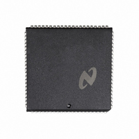
DP8344BV National Semiconductor, DP8344BV Datasheet - Page 29

DP8344BV
Manufacturer Part Number
DP8344BV
Description
IC BIPHASE COMM PROCESSR 84-PLCC
Manufacturer
National Semiconductor
Datasheet
1.DP8344BV.pdf
(184 pages)
Specifications of DP8344BV
Processor Type
8-Bit RISC
Speed
20MHz
Voltage
4.5 ~ 5.5V
Mounting Type
Surface Mount
Package / Case
84-PLCC
Operating Supply Voltage (typ)
5V
Operating Supply Voltage (max)
5.5V
Operating Supply Voltage (min)
4.5V
Mounting
Surface Mount
Operating Temperature (max)
70C
Operating Temperature (min)
0C
Operating Temperature Classification
Commercial
Lead Free Status / RoHS Status
Contains lead / RoHS non-compliant
Features
-
Lead Free Status / Rohs Status
Not Compliant
Other names
*DP8344BV
Available stocks
Company
Part Number
Manufacturer
Quantity
Price
Company:
Part Number:
DP8344BV
Manufacturer:
NSC
Quantity:
5 510
Part Number:
DP8344BV
Manufacturer:
NS/国半
Quantity:
20 000
2 0 CPU Description
Several conditions apply to these flags independent of their
operation and the way they are calculated These conditions
are
1 A flag’s previous state is retained when an instruction has
2 Direct reading and writing of all ALU flags is possible via
3 Currrent flag values are saved onto the address stack
4 Flag status is calculated in parallel with the instruction
When performing single byte arithmetic (i e the values are
completely represented in one byte) the Add (ADD ADDA)
and Subtract (SUB SUBA) instructions should be used but
when performing multi-byte arithmetic the Add with Carry
(ADCA) and Subtract with Carry (SBCA) instructions should
be used This is because the carry (in an add operation) or
the borrow (in a subtract operation) must be carried forward
to the higher order bytes Figure 2-11 demonstrates an in-
struction sequence for a 16-bit add and an instruction se-
quence for a 16-bit subtract
When using the ALU to perform comparisons the program-
mer has two options If the compare is to a constant value
then the CMP instruction can be used else one of the sub-
tract instructions must be used When determining the re-
sults of any compare the programmer must keep in mind
whether they are comparing signed or unsigned values Ta-
ble 2-22 lists the Boolean condition that must be met for
unsigned comparisons and Table 2-23 lists the Boolean
condition that must be met for signed comparisons
Assume the 16-bit variable X is represented by the reg-
ister pair R4(MSB) R5(LSB) and that the 16-bit variable
Y is represented by the register pair R6(MSB) R7(LSB)
To perform the assignment Y
To perform the assignment Y
no affect on that flag
the CCR register
during interrupt and call operations and can be restored
to their original values if a return instruction with the re-
store flags option is executed
result therefore no time penalty is associated with flag
operation
MOVE
ADDA
MOVE
ADCA
MOVE
SUBA
MOVE
SBCA
FIGURE 2-11 Multi-Byte Arithmetic
R7 A
R5 R7
R6 A
R4 R6
R7 A
R5 R7
R6 A
R4 R6
Instruction Sequences
GET LSB OF Y
Y(LSB) X(LSB) Y(LSB)
GET MSB OF Y
Y(MSB) X(MSB) Y(MSB)
GET LSB OF Y
Y(LSB) X(LSB) Y(LSB)
GET MSB OF Y
Y(MSB) X(MSB) Y(MSB)
CARRY
CARRY
e
e
(Continued)
X
X
a
Y
Y
29
Note
Note
2 2 2 Timing
Timing on the BCP is controlled by an internal oscillator and
circuitry that generates the internal timing signals This cir-
cuitry in the CPU is referred to as Timing Control The inter-
nal timing of the CPU is synchronized to an internal clock
called the CPU clock CPU-CLK A period of CPU-CLK is
referred to as a T-state The clock for the BCP is provided
by a crystal connected between X1 and X2 or from a clock
source connected to X1 This clock will be referred to as the
oscillator clock OCLK The frequency of OCLK is divided in
half when the CPU clock select bit
Control Register
OCLK 2 is used by Timing Control to generate CPU-CLK
and other synchronous signals used to control the CPU tim-
ing
After the BCP is reset CCS is high and CPU-CLK is gener-
ated from OCLK 2 Since the output of the divider that cre-
ates OCLK 2 can be high or low after reset CPU-CLK can
also be in a high or low state Therefore the exact number
of clock cycles to the start of the first instruction cannot be
determined Automatic test equipment can synchronize to
the BCP by asserting RESET as shown in Figure 2-12 The
falling edge of RESET generates a clear signal which caus-
es CPU-CLK to fall The next rising edge of X1 removes the
clear signal from CPU-CLK The second rising edge of X1
will cause CPU-CLK to rise and the relationship between X1
and CPU-CLK can be determined from this point
Writing a zero to CCS causes CPU-CLK to switch from
OCLK 2 to OCLK The transition from OCLK to OCLK 2
occurs following the end of the instruction that writes to
Comparison x
Comparison x
l
z
l
z
e
e
e
e
e
e
logical AND
logical AND
logical OR
logical OR
one’s complement
one’s complement
x
x
x
x
x
x
x
x
X
x
Unsigned Comparison Results
k
s
e
t
l
k
s
e
l
t
Signed Comparison Results
y
y
y
y
y
y
y
y
y
y
DCR
b
b
TABLE 2-22
y
TABLE 2-23
y
is set to a one Either OCLK or
Boolean Condition
Boolean Condition
(N V Z)
Z
(N V)
(N V)
l
CCS
(N V)
C
C
C
Z
C
Z
l
l
l
l
Z
(N V)
(N V)
(N V Z)
in the Device
Z
l
(N V)


