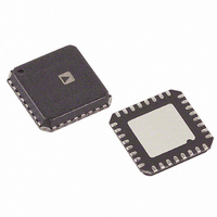
ADAU1361BCPZ Analog Devices Inc, ADAU1361BCPZ Datasheet - Page 73

ADAU1361BCPZ
Manufacturer Part Number
ADAU1361BCPZ
Description
IC CODEC 24B PLL 32LFCSP
Manufacturer
Analog Devices Inc
Type
Audio Codecr
Datasheet
1.ADAU1361BCPZ-RL.pdf
(80 pages)
Specifications of ADAU1361BCPZ
Data Interface
Serial
Resolution (bits)
24 b
Number Of Adcs / Dacs
2 / 2
Sigma Delta
No
Voltage - Supply, Analog
1.8 V ~ 3.6 V
Voltage - Supply, Digital
1.8 V ~ 3.6 V
Operating Temperature
-40°C ~ 85°C
Mounting Type
Surface Mount
Package / Case
32-VFQFN, CSP Exposed Pad
Audio Codec Type
Stereo
No. Of Adcs
2
No. Of Dacs
2
No. Of Input Channels
6
No. Of Output Channels
7
Adc / Dac Resolution
24bit
Adcs / Dacs Signal To Noise Ratio
101dB
Lead Free Status / RoHS Status
Lead free / RoHS Compliant
Available stocks
Company
Part Number
Manufacturer
Quantity
Price
Company:
Part Number:
ADAU1361BCPZ
Manufacturer:
TOSHIBA
Quantity:
1 650
Company:
Part Number:
ADAU1361BCPZ
Manufacturer:
ADI
Quantity:
624
Part Number:
ADAU1361BCPZ
Manufacturer:
ADI/亚德诺
Quantity:
20 000
Part Number:
ADAU1361BCPZ-R7
Manufacturer:
ADI/亚德诺
Quantity:
20 000
R42: Jack Detect Pin Control, 16,433 (0x4031)
With IOVDD set to 3.3 V, the low and high drive strengths of the JACKDET/MICIN pin are approximately 2.0 mA and 4.0 mA, respectively.
With IOVDD set to 1.8 V, the low and high drive strengths are approximately 0.8 mA and 1.7 mA, respectively. The optional pull-up/
pull-down resistors are nominally 250 kΩ. When enabled, these pull-up/pull-down resistors set the input signals to a defined state when
the signal source becomes three-state.
Bit 7
Table 69. Jack Detect Pin Control Register
Bits
5
[3:2]
R67: Dejitter Control, 16,438 (0x4036)
The dejitter control register allows the size of the dejitter window to be set, and also allows all dejitter circuits in the device to be activated or
bypassed. Dejitter circuits protect against duplicate samples or skipped samples due to jitter from the serial ports in slave mode. Disabling
and reenabling certain subsystems in the device—that is, the ADCs, serial ports, and DACs—during operation can cause the associated
dejitter circuits to fail. As a result, audio data fails to be output to the next subsystem in the device.
When the serial ports are in master mode, the dejitter circuit can be bypassed by setting the dejitter window to 0. When the serial ports
are in slave mode, the dejitter circuit can be reinitialized prior to outputting audio from the device, guaranteeing that audio is output
to the next subsystem in the device. Any time that audio must pass through the ADCs, serial port, or DACs, the dejitter circuit can be
bypassed and reset by setting the dejitter window size to 0. In this way, the dejitter circuit can be immediately reactivated, without a wait
period, by setting the dejitter window size to the default value of 3.
Bit 7
Table 70. Dejitter Control Register
Bits
[7:0]
Bit Name
JDSTR
JDP[1:0]
Bit Name
DEJIT[7:0]
Reserved
Bit 6
Bit 6
JACKDET/MICIN pin drive strength.
Description
0 = low (default).
1 = high.
JACKDET/MICIN pad pull-up/pull-down configuration.
Setting
00
01
10
11
Description
Dejitter window size.
Window Size
00000000
…
00000011
…
00000101
Bit 5
JDSTR
Bit 5
Bit 4
Reserved
Bit 4
Core Clock Cycles
0
…
3 (default)
…
5
Configuration
Pull-up
Reserved
None (default)
Pull-down
Rev. C | Page 73 of 80
DEJIT[7:0]
Bit 3
Bit 3
JDP[1:0]
Bit 2
Bit 2
Bit 1
Bit 1
Reserved
ADAU1361
Bit 0
Bit 0


