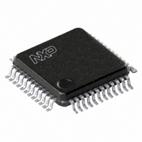
TDA8007BHL/C3,118 NXP Semiconductors, TDA8007BHL/C3,118 Datasheet - Page 7

TDA8007BHL/C3,118
Manufacturer Part Number
TDA8007BHL/C3,118
Description
IC INTERFACE CARD MP 48-LQFP
Manufacturer
NXP Semiconductors
Datasheet
1.TDA8007BHLC3118.pdf
(51 pages)
Specifications of TDA8007BHL/C3,118
Controller Type
Multiprotocol IC Card Interface
Interface
Parallel
Voltage - Supply
2.7 V ~ 6 V
Current - Supply
315mA
Operating Temperature
-40°C ~ 85°C
Mounting Type
Surface Mount
Package / Case
48-LQFP
Maximum Operating Temperature
+ 85 C
Minimum Operating Temperature
- 40 C
Mounting Style
SMD/SMT
Lead Free Status / RoHS Status
Lead free / RoHS Compliant
Other names
568-3520-2
935272525118
TDA8007BHLBE-T
935272525118
TDA8007BHLBE-T
Available stocks
Company
Part Number
Manufacturer
Quantity
Price
Company:
Part Number:
TDA8007BHL/C3,118
Manufacturer:
NXP Semiconductors
Quantity:
10 000
NXP Semiconductors
8. Functional description
TDA8007BHL
Product data sheet
8.1.1 Non-Multiplexed configuration
8.1 Interface control
Table 3.
Remark: Throughout this document, it is assumed that the reader is familiar with ISO7816
terminology.
The TDA8007BHL/C3 is sensitive to ESD in functional mode. This sensitivity is seen on
pin ALE: an electrostatic discharge causes an edge on this pin and changes its mode of
communication. When the mode of communication is the multiplexed mode, this has no
impact. But when the mode used is the non-multiplexed mode, the ESD may change the
mode to multiplexed mode, which is irreversible without power-off/power-on.
The TDA8007BHL/C4 is an evolution of the C3 version in which the communication mode
is set to non-multiplexed and can not be changed.
The TDA8007BHL/C4 is only in the non-multiplexed configuration
TDA8007BHL/C3 offers a multiplexed configuration in addition to a non-mulitplexed
configuration. The configuration can be chosen through the ALE-pin. If pin ALE is tied to
V
The TDA8007BHL can be controlled via an 12-bit parallel bus (bits D0 to D7 and bits A0 to
A3). The address bits are determined by means of pins AD0 to AD3. The read or write
control signal is on pin RD and a data write or read active low enable signal is on pin WR.
Signals CS and WR play the same role.
In read operations (see
chosen address is available on the bus when both signals CS and WR are low.
In write operations (see
is written when signals CS and WR are low.
In both configurations, the TDA8007BHL/C4 is selected only when signal CS = low.
Signal INT is an active low interrupt signal.
Symbol
AD0
XTAL2
XTAL1
DELAY
DD
or ground, the TDA8007BHL/C3 will be in the non-multiplexed configuration.
Pin description
All information provided in this document is subject to legal disclaimers.
Pin
45
46
47
48
Rev. 8 — 11 January 2011
Figure
Figure 5
…continued
4) with signal RD = high, the data corresponding to the
and 6) with signal RD = low, the data present on the bus
Description
register selection address 0 input
connection for an external crystal
connection for an external crystal or input for an
external clock signal
connection for an external delay capacitor
Multiprotocol IC card interface
TDA8007BHL
(Figure
© NXP B.V. 2011. All rights reserved.
3), where the
7 of 51


