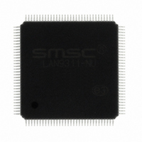
LAN9311-NU SMSC, LAN9311-NU Datasheet - Page 109

LAN9311-NU
Manufacturer Part Number
LAN9311-NU
Description
IC ETHER SW 2PRT 16BIT 128-VTQFP
Manufacturer
SMSC
Type
Two Port Managed Ethernet Switchr
Specifications of LAN9311-NU
Controller Type
Ethernet Switch Controller
Interface
Serial EEPROM
Voltage - Supply
3.3V
Operating Temperature
0°C ~ 70°C
Mounting Type
Surface Mount
Package / Case
128-TQFP, 128-VQFP
Product
Ethernet Switches
Number Of Transceivers
1
Standard Supported
802.3, 802.3u
Data Rate
10 MB, 100 MB
Supply Voltage (max)
3.3 V
Supply Voltage (min)
0 V
Maximum Operating Temperature
+ 70 C
Ethernet Connection Type
10 Base-T, 100 Base-TX
Minimum Operating Temperature
0 C
Mounting Style
SMD/SMT
For Use With
638-1076 - EVALUATION BOARD LAN9311-NU
Lead Free Status / RoHS Status
Lead free / RoHS Compliant
Current - Supply
-
Lead Free Status / Rohs Status
Lead free / RoHS Compliant
Other names
638-1075
Available stocks
Company
Part Number
Manufacturer
Quantity
Price
Company:
Part Number:
LAN9311-NU
Manufacturer:
CINCERA
Quantity:
3 023
Company:
Part Number:
LAN9311-NU
Manufacturer:
Microchip Technology
Quantity:
10 000
Part Number:
LAN9311-NU
Manufacturer:
SMSC
Quantity:
20 000
- Current page: 109 of 460
- Download datasheet (5Mb)
Two Port 10/100 Managed Ethernet Switch with 16-Bit Non-PCI CPU Interface
Datasheet
SMSC LAN9311/LAN9311i
8.5.6
D[15:0] (OUTPUT)
RX Data FIFO Direct PIO Reads
In this mode only A[2:1] are decoded, and any read of the LAN9311/LAN9311i will read the RX Data
FIFO. This mode is enabled when FIFO_SEL is driven high during a read access. This is normally
accomplished by connecting the FIFO_SEL signal to a high-order address line. This mode is useful
when the host processor must increment its address when accessing the LAN9311/LAN9311i.
Timing is identical to a PIO read and the FIFO_SEL and END_SEL signals have the same timing
characteristics as the address lines. An RX Data FIFO direct PIO read cycle begins when both nCS
and nRD are asserted. Either or both of these control signals must de-assert between cycles for the
period specified in
The cycle ends when either or both nCS and nRD are de-asserted. These signals may be asserted
and de-asserted in any order. Read data is valid as indicated in the functional timing diagram in
Figure
Note: Address lines A[2:1] are still used, and address lines A[9:3] are ignored.
Please refer to
AC timing specifications for RX Data FIFO direct PIO read operations.
Figure 8.5 Functional Timing for RX Data FIFO Direct PIO Read Operation
8.5.
END_SEL
FIFO_SEL
nCS, nRD
A[2:1]
A[x:3]
Section 15.5.6, "RX Data FIFO Direct PIO Read Cycle Timing," on page 449
Table 15.10, “RX Data FIFO Direct PIO Read Cycle Timing Values,” on page
(READ DATA FROM RX DATA FIFO)
DATASHEET
109
VALID
VALID
VALID
Revision 1.7 (06-29-10)
for the
449.
Related parts for LAN9311-NU
Image
Part Number
Description
Manufacturer
Datasheet
Request
R

Part Number:
Description:
Ethernet ICs Two Port 10/100 Ethernet Switch
Manufacturer:
SMSC
Datasheet:

Part Number:
Description:
FAST ETHERNET PHYSICAL LAYER DEVICE
Manufacturer:
SMSC Corporation
Datasheet:

Part Number:
Description:
357-036-542-201 CARDEDGE 36POS DL .156 BLK LOPRO
Manufacturer:
SMSC Corporation
Datasheet:

Part Number:
Description:
357-036-542-201 CARDEDGE 36POS DL .156 BLK LOPRO
Manufacturer:
SMSC Corporation
Datasheet:

Part Number:
Description:
357-036-542-201 CARDEDGE 36POS DL .156 BLK LOPRO
Manufacturer:
SMSC Corporation
Datasheet:

Part Number:
Description:
4-PORT USB2.0 HUB CONTROLLER
Manufacturer:
SMSC Corporation
Datasheet:

Part Number:
Description:
Manufacturer:
SMSC Corporation
Datasheet:

Part Number:
Description:
Manufacturer:
SMSC Corporation
Datasheet:

Part Number:
Description:
FDC37C672ENHANCED SUPER I/O CONTROLLER WITH FAST IR
Manufacturer:
SMSC Corporation
Datasheet:

Part Number:
Description:
COM90C66LJPARCNET Controller/Transceiver with AT Interface and On-Chip RAM
Manufacturer:
SMSC Corporation
Datasheet:

Part Number:
Description:
Manufacturer:
SMSC Corporation
Datasheet:

Part Number:
Description:
Manufacturer:
SMSC Corporation
Datasheet:

Part Number:
Description:
Manufacturer:
SMSC Corporation
Datasheet:

Part Number:
Description:
Manufacturer:
SMSC Corporation
Datasheet:


