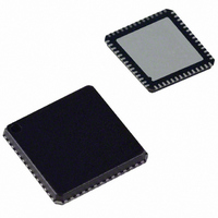
AD9911BCPZ Analog Devices Inc, AD9911BCPZ Datasheet - Page 11

AD9911BCPZ
Manufacturer Part Number
AD9911BCPZ
Description
IC DDS 500MSPS DAC 10BIT 56LFCSP
Manufacturer
Analog Devices Inc
Datasheet
1.AD9911BCPZ-REEL7.pdf
(44 pages)
Specifications of AD9911BCPZ
Resolution (bits)
10 b
Master Fclk
500MHz
Tuning Word Width (bits)
32 b
Voltage - Supply
1.71 V ~ 1.96 V
Operating Temperature
-40°C ~ 85°C
Mounting Type
Surface Mount
Package / Case
56-LFCSP
Transmitting Current
73mA
Data Rate
800Mbps
Rf Ic Case Style
LFCSP
No. Of Pins
56
Supply Voltage Range
1.71V To 1.89V, 3.135V To 3.465V
Operating Temperature Range
-40°C To +85°C
Msl
MSL 3 - 168 Hours
Lead Free Status / RoHS Status
Lead free / RoHS Compliant
For Use With
AD9911/PCBZ - BOARD EVAL FOR AD9911AD9911/PCB - BOARD EVAL FOR AD9911
Lead Free Status / Rohs Status
Compliant
Available stocks
Company
Part Number
Manufacturer
Quantity
Price
Company:
Part Number:
AD9911BCPZ
Manufacturer:
NXP
Quantity:
173
Part Number:
AD9911BCPZ
Manufacturer:
ADI/亚德诺
Quantity:
20 000
Pin No.
6, 10, 12, 16, 28, 32
40, 41, 42, 43
46
47
48
49
50
51, 52, 53
54
Mnemonic
NC
P0, P1, P2, P3
I/O_UPDATE
CS
SCLK
DVDD_I/O
SDIO_0
SDIO_1, SDIO_2,
SDIO_3
SYNC_CLK
N/A
I/O
O
I/O
I
I
I
I
I
I/O
Description
No Connection. Analog Devices recommends leaving these pins floating.
These data pins are used for modulation (FSK, PSK, ASK), start/stop for the sweep
accumulator, and ramping up/down the output amplitude. Any toggle of these data
inputs is equivalent to an I/O_UPDATE. The data is synchronous to the SYNC_CLK (Pin
54). The data inputs must meet the set-up and hold time requirements to the
SYNC_CLK. This guarantees a fixed pipeline delay of data to the DAC output;
otherwise, a ±1 SYNC_CLK period of uncertainty occurs. The functionality of these
pins is controlled by profile pin configuration (PPC) bits in Register FR1 <12:14>.
A rising edge triggers data transfer from the I/O port buffer to active registers.
I/O_UPDATE is synchronous to the SYNC_CLK (Pin 54). I/O_UPDATE must meet the
set-up and hold time requirements to the SYNC_CLK to guarantee a fixed pipeline
delay of data to DAC output. If not, a ±1 SYNC_CLK period of uncertainty occurs. The
minimum pulse width is one SYNC_CLK period.
The active low chip select allows multiple devices to share a common I/O bus (SPI).
Data Clock for I/O Operations. Data bits are written on the rising edge of SCLK and
read on the falling edge of SCLK.
3.3 V Digital Power Supply for SPI Port and Digital I/O.
Data pin SDIO_0 is dedicated to the I/O port only.
Data pins SDIO_1:3 can be used for the I/O port or to initiate a ramp up/ramp down
(RU/RD) of the DAC output amplitude.
The SYNC_CLK, which runs at ¼ the system clock rate, can be disabled. I/O_UPDATE
and profile changes (Pin 40 to Pin 43) are synchronous to the SYNC_CLK. To guarantee
a fixed pipeline delay of data to DAC output, I/O_UPDATE and profile changes (Pin 40
to Pin 43) must meet the set-up and hold time requirements to the rising edge of
SYNC_CLK. If not, a ±1 SYNC_CLK period of uncertainty exists.
Rev. 0 | Page 11 of 44
AD9911


