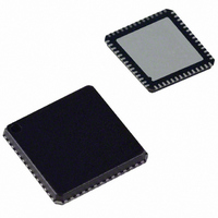
AD9911BCPZ Analog Devices Inc, AD9911BCPZ Datasheet - Page 24

AD9911BCPZ
Manufacturer Part Number
AD9911BCPZ
Description
IC DDS 500MSPS DAC 10BIT 56LFCSP
Manufacturer
Analog Devices Inc
Datasheet
1.AD9911BCPZ-REEL7.pdf
(44 pages)
Specifications of AD9911BCPZ
Resolution (bits)
10 b
Master Fclk
500MHz
Tuning Word Width (bits)
32 b
Voltage - Supply
1.71 V ~ 1.96 V
Operating Temperature
-40°C ~ 85°C
Mounting Type
Surface Mount
Package / Case
56-LFCSP
Transmitting Current
73mA
Data Rate
800Mbps
Rf Ic Case Style
LFCSP
No. Of Pins
56
Supply Voltage Range
1.71V To 1.89V, 3.135V To 3.465V
Operating Temperature Range
-40°C To +85°C
Msl
MSL 3 - 168 Hours
Lead Free Status / RoHS Status
Lead free / RoHS Compliant
For Use With
AD9911/PCBZ - BOARD EVAL FOR AD9911AD9911/PCB - BOARD EVAL FOR AD9911
Lead Free Status / Rohs Status
Compliant
Available stocks
Company
Part Number
Manufacturer
Quantity
Price
Company:
Part Number:
AD9911BCPZ
Manufacturer:
NXP
Quantity:
173
Part Number:
AD9911BCPZ
Manufacturer:
ADI/亚德诺
Quantity:
20 000
AD9911
Setting the Rate of the Linear Sweep
The rate of the linear sweep is set by the intermediate step size
(delta-tuning word) between S0 and E0 (see Figure 42) and the
time spent (sweep ramp rate word) at each step. The resolution
of the delta-tuning word is 32 bits for frequency, 14 bits for
phase, and 10 bits for amplitude. The resolution for the delta
ramp rate word is 8 bits.
In linear sweep, the user programs a rising delta word (RDW,
Register 0x08) and a rising sweep ramp rate word (RSRR,
Register 0x07). These settings apply when sweeping from F0 to
E0. The falling delta word (FDW, Register 0x09) and falling
sweep ramp rate (FSRR, Register 0x07) apply when sweeping
from E0 to S0.
When programming, note that attention is required to prevent
overflow of the sweep. If the sweep accumulator is allowed to
overflow, an uncontrolled, continuous sweep operation occurs.
To avoid this, the magnitude of the rising or falling delta word
should be smaller than the difference between full scale and the
E0 value (full scale − E0). For a frequency sweep, full scale is
2
sweep, full scale is 2
The graph in Figure 42 displays a linear sweep up and then
down using a profile pin. Note that the no dwell bit is cleared. If
the no dwell bit (CFR<15>) is set, the sweep accumulator
returns to 0 upon reaching E0. For more information, see the
Linear Sweep No Dwell Mode section.
31
−1. For a phase sweep, full scale is 2
EO
SO
Δf,p,a
RDW
PROFILE PIN
Figure 42. Linear Sweep Mode
10
FREQ SWEEP EN
−1.
Δt
RSRR
TIME
CTW0
0
MUX
FSRR
14
1
−1. For an amplitude
ACCUMULATOR
Δt
PHASE
FDW
PHASE SWEEP EN
Z
Δf,p,a
–1
Figure 41. Linear Sweep Capability
Rev. 0 | Page 24 of 44
32
PHASE OFFSET
CPW0
0
ADDER
MUX
SWEEP FUNCTION LOGIC
1
For a piecemeal or a nonlinear transition between S0 and E0,
the delta tuning words and ramp rate words can be repro-
grammed during the transition.
The formulae for calculating the step size of RDW or FDW are
The formula for calculating delta time from RSRR or FSRR is
At 500 MSPS operation (SYNC_CLK =125 MHz), the
minimum time interval between steps is 1/125 MHz × 1 = 8 ns.
The maximum time interval is (1/125 MHz) × 255 = 2.04 μs.
Frequency Linear Sweep Example
This section provides an example of a frequency linear sweep
followed by a description.
AFP CFR<23:22> =10, modulation level FR1<9:8> = 00, sweep
enable CFR<14> = 1, linear sweep no-dwell CFR<15> = 0.
In linear sweep mode, when the profile pin transitions from low
to high, the RDW is applied to the input of the sweep accumu-
lator and the RSRR register is loaded into the sweep rate timer.
The RDW accumulates at the rate given by the ramp rate
(RSRR) until the output equals the CTW1 register value. The
sweep is then complete and the output held constant in
frequency.
When the profile pin transitions from high to low, the FDW is
applied to the input of the sweep accumulator and the FSRR
register is loaded into the sweep rate timer.
The FDW accumulates at the rate given by the ramp rate
(FSRR) until the output equals the CTW0 register value. The
15
Δ
Δ
Δ
ΔΦ
a
f
t =
AMP SWEEP EN
=
COS(X)
=
=
⎛
⎜
⎝
(
⎛
⎜
⎝
⎛
⎜
⎝
RSRR
RDW
RDW
2
RDW
2
10
2
32
14
⎞
⎟
⎠
)
/
×
⎞
⎟
⎠
⎞
⎟
⎠
SYNC
10
×
ACR
×
DAC full-scale current
0
SYNC
360
MUX
°
_
RU/RD LOGIC
CLK
1
_
CLK
(
Hz
(Hz)
DAC
)


