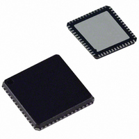
AD9911BCPZ Analog Devices Inc, AD9911BCPZ Datasheet - Page 23

AD9911BCPZ
Manufacturer Part Number
AD9911BCPZ
Description
IC DDS 500MSPS DAC 10BIT 56LFCSP
Manufacturer
Analog Devices Inc
Datasheet
1.AD9911BCPZ-REEL7.pdf
(44 pages)
Specifications of AD9911BCPZ
Resolution (bits)
10 b
Master Fclk
500MHz
Tuning Word Width (bits)
32 b
Voltage - Supply
1.71 V ~ 1.96 V
Operating Temperature
-40°C ~ 85°C
Mounting Type
Surface Mount
Package / Case
56-LFCSP
Transmitting Current
73mA
Data Rate
800Mbps
Rf Ic Case Style
LFCSP
No. Of Pins
56
Supply Voltage Range
1.71V To 1.89V, 3.135V To 3.465V
Operating Temperature Range
-40°C To +85°C
Msl
MSL 3 - 168 Hours
Lead Free Status / RoHS Status
Lead free / RoHS Compliant
For Use With
AD9911/PCBZ - BOARD EVAL FOR AD9911AD9911/PCB - BOARD EVAL FOR AD9911
Lead Free Status / Rohs Status
Compliant
Available stocks
Company
Part Number
Manufacturer
Quantity
Price
Company:
Part Number:
AD9911BCPZ
Manufacturer:
NXP
Quantity:
173
Part Number:
AD9911BCPZ
Manufacturer:
ADI/亚德诺
Quantity:
20 000
Table 13. 2-Level Modulation—RU/RD
Profile Pin Config. Bits
FR1<14:12>
0
0
8-Level Modulation Using a Profile Pin for RU/RD
When the RU/RD bits = 10, Profile Pin P3 is available for
RU/RD. Note that only a modulation level of eight is available
when the RU/RD bits = 10. See Table 14 for available pin
assignments.
Table 14. 8-Level Modulation—RU/RD
Profile Pin Config. Bits FR1
<14:12>
x
SHIFT KEYING MODULATION USING SDIO PINS
FOR RU/RD
For RU/RD bits = 11, SDIO Pin 1, Pin 2, and Pin 3 are available
for RU/RD. In this mode, modulation levels of 2, 4, and 16 are
available. Note that the I/O port can only be used in 1-bit serial
mode.
Table 15. 2-Level Modulation Using SDIO Pins for RU/RD
Profile Pin Config. Bits
FR1 <14:12>
x
In this case, the SDIO pins can be used for the RU/RD function,
as described in Table 16.
Table 16. SDIO Pins
1
0
0
4-Level Modulation Using SDIO Pins for RU/RD
For RU/RD = 11 (SDIO Pin 1 and Pin 2 are available for
RU/RD), the modulation level is set to four. See Table 17 for pin
assignments, including SDIO pin assignments.
Table 17.
Profile Pin
Config. Bits
(FR1<14:12>)
0
0
For the configuration shown in Table 17, the profile register is
chosen based on the 2-bit value presented to <P0:P1> or
<P2:P3>. For example, if PPC = 011, <P0:P1> = 11, then the
contents of Profile Register 3 (Register 0x0C) are presented to
CH1 output. SDIO Pin 1 and Pin 2 provide the RU/RD function.
2
1
1
0
1
0
1
3
0
1
x
0
1
0
P0
N/A
CH1
Description
Triggers the ramp-up function for CH1
Triggers the ramp-down function for CH1
P1
N/A
CH1
x
0
1
1
P2
CH1
N/A
P0
N/A
P3
CH1
N/A
P0
N/A
CH1
P0
CH1
SDIO_1
N/A
CH1
RU/RD
P1
CH1
P1
CH1
N/A
P1
CH1
P2
N/A
CH1
RU/RD
SDIO_2
CH1
RU/RD
N/A
P2
N/A
P2
CH1
P3
CH1
RU/RD
N/A
P3
CH1
RU/RD
P3
N/A
SDIO_3
N/A
N/A
Rev. 0 | Page 23 of 44
16-Level Modulation Using SDIO Pins for RU/RD
RU/RD = 11 (SDIO Pin 1 available for RU/RD) and the level is
set to 16. See the pin assignment shown in Table 18.
Table 18.
Profile Pin
Config. Bits
(FR1<14:12>)
x
For the configuration shown in Table 18, the profile register is
chosen based on the 4-bit value presented to <P0:P3>. For
example, if PPC = x01 and <P0:P3> = 1101, then the contents of
Profile Register 13 (Register 0x16) are presented to CH1 output.
The SDIO_1 pin provides the RU/RD function.
LINEAR SWEEP (SHAPED) MODULATION MODE
Linear sweep enables the user to sweep frequency, phase, or
amplitude from a starting point (S0) to an endpoint (E0). The
purpose of linear sweep mode is to provide better bandwidth
containment compared to direct modulation mode by enabling
more gradual, user-defined changes between S0 and E0. Note
that SYNC_CLK must be enabled when using Linear Sweep
while the auxiliary DDS cores must be disabled. Digital power
down (CSR bit <7>) of the auxiliary channels is recommended.
Figure 41 depicts the linear sweep block diagram.
In linear sweep mode, S0 is loaded into Profile Register 0
(Profile 0 is represented by Register 0x04, Register 0x05, or
Register 0x06, depending on the parameter being swept) and E0
is always loaded into Profile Register 1 (Register 0x0A). If E0 is
configured for frequency sweep, the resolution is 32-bits. For
phase sweep, the resolution is 14 bits and for amplitude sweep,
the resolution is 10 bits. When sweeping phase or amplitude,
the word value must be MSB-aligned in Profile Register 1;
unused bits are ignored. Profile Pin1 triggers and controls the
direction (up/down) of the linear sweep for frequency, phase, or
amplitude.
The AD9911 can be programmed to ramp up or ramp down the
output amplitude (using the 10-bit output scalar) before and
after a linear sweep. If the RU/RD feature is desired, profile pins
or SDIO_1:3 pins can be configured to control the RU/RD
operation. For further details, refer to the Output Amplitude
Control section. To enable linear sweep mode, AFP bits (CFR
<23:22>), modulation level bits (FR1 <9:8>), and the linear
sweep enable bit (CFR <14>) must be programmed. The AFP
bits determine the type of linear sweep to be performed (see
Table 19). The modulation level bits must be set to 00 (2-level).
Table 19.
AFP
CFR <23:22>
0
0
1
1
0
0
1
0
1
1
P0
CH1
Linear Sweep Enable
CFR <14>
1
1
1
1
P1
CH1
P2
CH1
P3
CH1
SDIO_1
CH1
RU/RD
Description
N/A
Amplitude sweep
Frequency sweep
Phase sweep
SDIO_2
N/A
AD9911
SDIO_3
N/A


