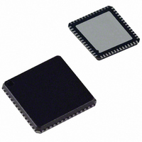
AD9911BCPZ Analog Devices Inc, AD9911BCPZ Datasheet - Page 38

AD9911BCPZ
Manufacturer Part Number
AD9911BCPZ
Description
IC DDS 500MSPS DAC 10BIT 56LFCSP
Manufacturer
Analog Devices Inc
Datasheet
1.AD9911BCPZ-REEL7.pdf
(44 pages)
Specifications of AD9911BCPZ
Resolution (bits)
10 b
Master Fclk
500MHz
Tuning Word Width (bits)
32 b
Voltage - Supply
1.71 V ~ 1.96 V
Operating Temperature
-40°C ~ 85°C
Mounting Type
Surface Mount
Package / Case
56-LFCSP
Transmitting Current
73mA
Data Rate
800Mbps
Rf Ic Case Style
LFCSP
No. Of Pins
56
Supply Voltage Range
1.71V To 1.89V, 3.135V To 3.465V
Operating Temperature Range
-40°C To +85°C
Msl
MSL 3 - 168 Hours
Lead Free Status / RoHS Status
Lead free / RoHS Compliant
For Use With
AD9911/PCBZ - BOARD EVAL FOR AD9911AD9911/PCB - BOARD EVAL FOR AD9911
Lead Free Status / Rohs Status
Compliant
Available stocks
Company
Part Number
Manufacturer
Quantity
Price
Company:
Part Number:
AD9911BCPZ
Manufacturer:
NXP
Quantity:
173
Part Number:
AD9911BCPZ
Manufacturer:
ADI/亚德诺
Quantity:
20 000
AD9911
CONTROL REGISTER DESCRIPTIONS
CHANNEL SELECT REGISTER (CSR)
The CSR register determines if channels are enabled or disabled
by the status of the channel enable bits. Channels are enabled by
default. The CSR register also determines which mode and
format (MSB-first or LSB-first) of operation is active.
The CSR is comprised of one byte located in Register 0x00.
CSR <0> LSB-first
CSR <0> = 0 (default), the serial interface, accepts data in MSB-
first format. CSR <0> = 1, the interface, accepts data in LSB-
first format.
CSR <2:1> I/O mode select
CSR <2:1> 00 = single bit serial (2-wire mode).
See the I/O Modes of Operation section for more details.
CSR <3> = must be cleared to 0.
CSR <7:4> channel enable bits.
CSR <7:4> bits are active immediately once written. They do
not require an I/O update to take effect.
There are four sets of channel registers and profile registers, one
per channel. This is not shown in the channel or profile register
map. The addresses of all channel registers and profile registers
are the same for each channel. Therefore, the channel enable
bits distinguish the channel registers and profile registers values
for each channel.
For example,
CSR <7:4> = 0010, only primary Channel 1 receives commands
from the channel and profile registers.
CSR <7:4> = 0000, only auxiliary Channel 0 receives commands
from the channel registers and profile registers.
CSR <7:4> = 0011, both Channel 0 and Channel 1 receive
commands from the channel registers and profile registers.
Function Register 1 (FR1) Description
FR1 is comprised of three bytes located in Register 0x01. The
FR1 is used to control the mode of operation of the chip. The
functionality of each bit is detailed as follows:
FR1 <0> manual software synchronization bit.
FR1 <0> = 0 (default), the software manual synchronization
feature is inactive. FR1 <0> = 1.The manual software
01 = single bit serial (3-wire mode).
10 = 2-bit mode.
11 = 4-bit mode.
Rev. 0 | Page 38 of 44
synchronization feature is active. See Synchronizing Multiple
AD9911 Devices section for details.
FR1 <1> Manual hardware synchronization bit.
FR1 <1> = 0 (default), the manual hardware synchronization
feature is inactive. FR1 <1> = 1, the manual hardware
synchronization feature is active. See the Synchronizing
Multiple AD9911 Devices +section for details.
FR1 <2> Test-tone modulation enable.
FR1 <2> = 0 (default) disables and 1 enables.
FR1 <3> open.
FR1 <4> DAC reference power-down.
FR1 <4> = 0 (default). The DAC reference is enabled.
FR1 <4> = 1. DAC reference is disabled and powered down.
FR1 <5> SYNC_CLK disable.
FR1 <5> = 0 (default), the SYNC_CLK pin is active.
FR1 <5> = 1. The SYNC_CLK pin assumes a static Logic 0
state (disabled). The pin drive logic is shut down. The
synchronization circuitry remains active internally (necessary
for normal device operation.)
FR1 <6> external power-down mode.
FR1 <6> = 0 (default). The external power-down mode is in the
fast recovery power-down mode. When the PWR_DWN_CTL
input pin is high, the digital logic and the DAC digital logic are
powered down. The DACs bias circuitry, PLL, oscillator, and
clock input circuitry are not powered down.
FR1 <6> = 1. The external power down mode is in the full
power-down mode. When the PWR_DWN_CTL input pin is
high, all functions are powered down. This includes the DAC
and PLL, which take a significant amount of time to power up.
FR1 <7> clock input power-down.
FR1 <7> = 0 (default). The clock input circuitry is enabled for
operation. FR1 <7> = 1. The clock input circuitry is disabled
and is in a low power dissipation state.
FR1 <9:8> modulation level bits.
The modulation (FSK, PSK, and ASK) level bits control the level
(2/4/8/16) of modulation to be performed. See Table 7 for
settings.
FR1 <11:10> RU/RD bits.
The RU/RD bits control how the profile pins and SDIO_1:3 pins
are assigned. See Table 8 for settings


