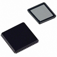
AD9911BCPZ Analog Devices Inc, AD9911BCPZ Datasheet - Page 39

AD9911BCPZ
Manufacturer Part Number
AD9911BCPZ
Description
IC DDS 500MSPS DAC 10BIT 56LFCSP
Manufacturer
Analog Devices Inc
Datasheet
1.AD9911BCPZ-REEL7.pdf
(44 pages)
Specifications of AD9911BCPZ
Resolution (bits)
10 b
Master Fclk
500MHz
Tuning Word Width (bits)
32 b
Voltage - Supply
1.71 V ~ 1.96 V
Operating Temperature
-40°C ~ 85°C
Mounting Type
Surface Mount
Package / Case
56-LFCSP
Transmitting Current
73mA
Data Rate
800Mbps
Rf Ic Case Style
LFCSP
No. Of Pins
56
Supply Voltage Range
1.71V To 1.89V, 3.135V To 3.465V
Operating Temperature Range
-40°C To +85°C
Msl
MSL 3 - 168 Hours
Lead Free Status / RoHS Status
Lead free / RoHS Compliant
For Use With
AD9911/PCBZ - BOARD EVAL FOR AD9911AD9911/PCB - BOARD EVAL FOR AD9911
Lead Free Status / Rohs Status
Compliant
Available stocks
Company
Part Number
Manufacturer
Quantity
Price
Company:
Part Number:
AD9911BCPZ
Manufacturer:
NXP
Quantity:
173
Part Number:
AD9911BCPZ
Manufacturer:
ADI/亚德诺
Quantity:
20 000
FR1 <12:14> profile pin configuration bits.
The profile pin configuration bits assign the profile and SDIO
pins for the different tasks. See the Shift Keying Modulation
section for examples.
FR1 <15> inactive.
FR1 <17:16> charge pump current control.
FR1 <17:16> = 00 (default), the charge pump current is 75 μA.
FR1 <22:18> PLL divider values.
FR1 <22:18>, if the value is > 3 and < 21, the PLL is enabled and
the value sets the multiplication factor. If the value is < 4 or >20
the PLL is disabled.
FR1 <23> PLL VCO gain.
FR1 <23> = 0 (default), the low range (system clock below
160 MHz). FR1 <23> = 1, the high range (system clock above
255 MHz).
Function Register 2 (FR2) Description
The FR2 is comprised of two bytes located in Address 0x02.
The FR2 is used to control the various functions, features, and
modes of the AD9911. The functionality of each bit is as
follows:
FR2<1:0> system clock offset. See the Synchronizing Multiple
AD9911 Devices section for more details.
FR2 <3:2> inactive.
FR2 <4:7>. Multidevice synchronization bits. See the
Synchronizing Multiple AD9911 Devices section for more
details.
FR2 <11:8> inactive.
FR2 <12> Clear phase accumulator.
FR2 <12> = 0 (default), the phase accumulator functions as
normal. FR2 <12> = 1, the phase accumulator memory
elements are asynchronously cleared.
FR2 <13> Auto clear phase accumulator.
FR2 <13> = 0 (default). A new frequency tuning word is applied
to the inputs of the phase accumulator, but not loaded into the
accumulator.
FR2 <13> = 1. This bit automatically synchronously clears
(loads zeros into) the phase accumulator for one cycle upon
reception of the I/O update sequence indicator on both
channels.
= 01 charge pump current is 100 μA.
= 10 charge pump current is 125 μA.
= 11 charge pump current is 150 μA.
Rev. 0 | Page 39 of 44
FR2 <14> Clear sweep accumulator.
FR2 <14> = 0 (default), the sweep accumulator functions as
normal. FR2 <14> = 1, the sweep accumulator memory
elements are asynchronously cleared.
FR2 <15> Auto clear sweep accumulator.
FR2 <15> = 0 (default). A new delta word is applied to the
input, as in normal operation, but not loaded into the accumu-
lator. FR2 <15> = 1. This bit automatically synchronously clears
(loads 0s) the sweep accumulator for one cycle upon reception
of the I/O_UPDATE sequence indicator on both channels.
CHANNEL FUNCTION REGISTER (CFR)
DESCRIPTION
CFR <0> Enable sine function.
CFR <0> = 0 (default). The angle-to-amplitude conversion logic
employs a cosine function. CFR <0> = 1. The angle-to-
amplitude conversion logic employs a sine function.
CFR <1> Clear phase accumulator.
CFR <1> = 0 (default). The phase accumulator functions as
normal. CFR <1> = 1. The phase accumulator memory
elements are asynchronously cleared.
CFR <2> auto clear phase accumulator.
CFR <2> = 0 (default). A new frequency tuning word is applied
to the inputs of the phase accumulator, but not loaded into the
accumulator. CFR <2> = 1. This bit automatically synchro-
nously clears (loads 0s) the phase accumulator for one cycle
upon reception of the I/O_UPDATE sequence indicator.
CFR <3> clear sweep accumulator.
CFR <3> = 0 (default). The sweep accumulator functions as
normal. CFR <3> = 1. The sweep accumulator memory
elements are asynchronously cleared.
CFR <4> auto clear sweep accumulator.
CFR <4> = 0 (default). A new delta word is applied to the input,
as in normal operation, but not loaded into the accumulator.
CFR <4> = 1. This bit automatically synchronously clears (loads
0s) the sweep accumulator for one cycle upon reception of the
I/O_UPDATE sequence indicator.
CFR <5> match pipe delays active.
CFR <5> = 0 (default), match pipe delay mode is inactive.
CFR <5> = 1, match pipe delay mode is active. See the Single-
Tone Mode—Matched Pipeline Delay section for details.
CFR <6> DAC power-down.
AD9911


