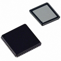
AD9911BCPZ Analog Devices Inc, AD9911BCPZ Datasheet - Page 3

AD9911BCPZ
Manufacturer Part Number
AD9911BCPZ
Description
IC DDS 500MSPS DAC 10BIT 56LFCSP
Manufacturer
Analog Devices Inc
Datasheet
1.AD9911BCPZ-REEL7.pdf
(44 pages)
Specifications of AD9911BCPZ
Resolution (bits)
10 b
Master Fclk
500MHz
Tuning Word Width (bits)
32 b
Voltage - Supply
1.71 V ~ 1.96 V
Operating Temperature
-40°C ~ 85°C
Mounting Type
Surface Mount
Package / Case
56-LFCSP
Transmitting Current
73mA
Data Rate
800Mbps
Rf Ic Case Style
LFCSP
No. Of Pins
56
Supply Voltage Range
1.71V To 1.89V, 3.135V To 3.465V
Operating Temperature Range
-40°C To +85°C
Msl
MSL 3 - 168 Hours
Lead Free Status / RoHS Status
Lead free / RoHS Compliant
For Use With
AD9911/PCBZ - BOARD EVAL FOR AD9911AD9911/PCB - BOARD EVAL FOR AD9911
Lead Free Status / Rohs Status
Compliant
Available stocks
Company
Part Number
Manufacturer
Quantity
Price
Company:
Part Number:
AD9911BCPZ
Manufacturer:
NXP
Quantity:
173
Part Number:
AD9911BCPZ
Manufacturer:
ADI/亚德诺
Quantity:
20 000
GENERAL DESCRIPTION
The DDS acts as a high resolution frequency divider with the
REF_CLK as the input and the DAC providing the output. The
REF_CLK input can be driven directly or used in combination
with an integrated REF_CLK multiplier (PLL). The REF_CLK
input also features an oscillator circuit to support an external
crystal as the REF_CLK source. The crystal can be used in
combination with the REF_CLK multiplier.
The AD9911 I/O port offers multiple configurations to provide
significant flexibility. The I/O port offers an SPI-compatible
mode of operation that is virtually identical to the SPI operation
found in earlier Analog Devices DDS products.
I/O_UPDATE
SYNC_OUT
SYNC_CLK
REF_CLK
REF_CLK
SYNC_IN
CLK_MODE_SEL
AD9911
OSCILLATOR
ΔFTW
32
FTW/
BUFFER/
XTAL
÷4
Σ
32
LOOP FILTER
MULTIPLIER
REF CLOCK
32
4× TO 20×
FUNCTIONAL BLOCK DIAGRAM
Σ
ΔPHASE
PHASE/
TIMING AND CONTROL LOGIC
Figure 2. Functional Block Diagram
Σ
AVDD
1.8V
14
SYSTEM
Rev. 0 | Page 3 of 44
15
CLK
MUX
COS(X)
DVDD
1.8V
CORE
DDS
Flexibility is provided by four data pins (Pin SDIO_0,
Pin SDIO_1, Pin SDIO_2, and Pin SDIO_3) that allow four
programmable modes of I/O operation.
The DAC output is supply referenced and must be terminated
into AVDD by a resistor and an AVDD center-tapped trans-
former. The DAC has its own programmable reference to enable
different full-scale currents.
The DDS core (the AVDD pins and the DVDD pins) is powered
by a 1.8 V supply. The digital I/O interface (SPI) operates at
3.3 V and requires that the Pin DVDD_I/O (Pin 49) be
connected to 3.3 V.
10
ΔAMP
AMP/
MUX
P0 P1
10
REGISTERS
REGISTERS
SPURKILLER/
10
MULTI-TONE
CONTROL
PROFILE
CORE
DDS
Σ
P2
CORE
P3
DDS
DVDD_I/O
BUFFER
SCALABLE
CURRENT
DAC REF
PORT
I/O
DAC
3.3V
IOUT
IOUT
DAC_RSET
PWR_DWN_CTL
MASTER_RESET
SCLK
CS
SDIO_0
SDIO_1
SDIO_2
SDIO_3
AD9911


