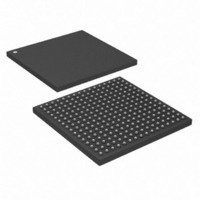
DS26518GN+ Maxim Integrated Products, DS26518GN+ Datasheet - Page 157

DS26518GN+
Manufacturer Part Number
DS26518GN+
Description
IC TXRX T1/E1/J1 8PORT 256-CSBGA
Manufacturer
Maxim Integrated Products
Type
Transceiverr
Specifications of DS26518GN+
Number Of Drivers/receivers
8/8
Protocol
T1/E1/J1
Voltage - Supply
3.135 V ~ 3.465 V
Mounting Type
Surface Mount
Package / Case
256-CSBGA
Lead Free Status / RoHS Status
Lead free / RoHS Compliant
- Current page: 157 of 286
- Download datasheet (2Mb)
Register Name:
Register Description:
Register Address:
Bit #
Name
Default
Bit 6: u-Law or A-Law Digital Milliwatt Code Select (uALAW)
Bit 5: RSERn Control (RSERC)
Bits 4 and 3: Receive Bit Inversion (BINV[1:0])
Bit 1: Payload Loopback (PLB)
When PLB is enabled, the following will occur:
In a PLB situation, the DS26518 will loop the 192 bits (248 for E1) of payload data (with BPVs corrected) from the
receive section back to the transmit section. The transmitter will follow the frame alignment provided by the
receiver. The receive frame boundary is automatically fed into the transmit section, such that the transmit frame
position is locked to the receiver (i.e., TSYNCn is sourced from RSYNCn). The FPS framing pattern, CRC-6
calculation, and the FDL bits (FAS word, Si, Sa, E bits, and CRC-4 for E1) are not looped back, they are reinserted
by the DS26518 (i.e., the transmit section will modify the payload as if it was input at TSERn).
Bit 0: Framer Loopback (FLB)
This loopback is useful in testing and debugging applications. In FLB, the DS26518 will loop data from the transmit
side back to the receive side. When FLB is enabled, the following will occur:
1) Data will be transmitted on TTIPn and TRINGn synchronous with RCLKn instead of TCLKn.
2) All of the receive-side signals will continue to operate normally.
3) The TCHCLKn and TCHBLKn signals are forced low.
4) Data at the TSERn, TDATAn, and TSIGn pins is ignored.
0 = u-law code is inserted based on T1RDMWE1–3 or E1RDMWE1–4 registers.
1 = A-law code is inserted based on T1RDMWE1–3 or E1RDMWE1–4 registers.
0 = Allow RSERn to output data as received under all conditions (normal operation).
1 = Force RSERn to one under loss of frame alignment conditions.
00 = No inversion.
01 = Invert framing.
10 = Invert signaling.
11 = Invert payload.
0 = Loopback disabled.
1 = Loopback enabled.
0 = loopback disabled
1 = loopback enabled
1) (T1 mode) an unframed all-ones code will be transmitted at TTIPn and TRINGn.
2) Data at RTIPn and RRINGn will be ignored.
3) All receive-side signals will take on timing synchronous with TCLKn instead of RCLKn.
Note that it is not acceptable to have RCLKn tied to TCLKn during this loopback because this will cause an
unstable condition.
(E1 mode) normal data will be transmitted at TTIPn and TRINGn.
—
7
0
RCR3
Receive Control Register 3
083h + (200h x (n - 1)) : where n = 1 to 8
uALAW
6
0
RSERC
5
0
157 of 286
BINV1
4
0
BINV0
3
0
DS26518 8-Port T1/E1/J1 Transceiver
—
2
0
PLB
1
0
FLB
0
0
Related parts for DS26518GN+
Image
Part Number
Description
Manufacturer
Datasheet
Request
R

Part Number:
Description:
8-port T1/e1/j1 Transceiver
Manufacturer:
Maxim Integrated Products, Inc.
Datasheet:

Part Number:
Description:
Ds26518 8-port T1/e1/j1 Transceiver
Manufacturer:
Maxim Integrated Products, Inc.

Part Number:
Description:
power light source LUXEON� Collimator
Manufacturer:
LUMILEDS [Lumileds Lighting Company]
Datasheet:

Part Number:
Description:
MAX7528KCWPMaxim Integrated Products [CMOS Dual 8-Bit Buffered Multiplying DACs]
Manufacturer:
Maxim Integrated Products
Datasheet:

Part Number:
Description:
Single +5V, fully integrated, 1.25Gbps laser diode driver.
Manufacturer:
Maxim Integrated Products
Datasheet:

Part Number:
Description:
Single +5V, fully integrated, 155Mbps laser diode driver.
Manufacturer:
Maxim Integrated Products
Datasheet:

Part Number:
Description:
VRD11/VRD10, K8 Rev F 2/3/4-Phase PWM Controllers with Integrated Dual MOSFET Drivers
Manufacturer:
Maxim Integrated Products
Datasheet:

Part Number:
Description:
Highly Integrated Level 2 SMBus Battery Chargers
Manufacturer:
Maxim Integrated Products
Datasheet:

Part Number:
Description:
Current Monitor and Accumulator with Integrated Sense Resistor; ; Temperature Range: -40°C to +85°C
Manufacturer:
Maxim Integrated Products

Part Number:
Description:
TSSOP 14/A�/RS-485 Transceivers with Integrated 100O/120O Termination Resis
Manufacturer:
Maxim Integrated Products

Part Number:
Description:
TSSOP 14/A�/RS-485 Transceivers with Integrated 100O/120O Termination Resis
Manufacturer:
Maxim Integrated Products

Part Number:
Description:
QFN 16/A�/AC-DC and DC-DC Peak-Current-Mode Converters with Integrated Step
Manufacturer:
Maxim Integrated Products

Part Number:
Description:
TDFN/A/65V, 1A, 600KHZ, SYNCHRONOUS STEP-DOWN REGULATOR WITH INTEGRATED SWI
Manufacturer:
Maxim Integrated Products

Part Number:
Description:
Integrated Temperature Controller f
Manufacturer:
Maxim Integrated Products


