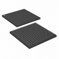
DS26518GN+ Maxim Integrated Products, DS26518GN+ Datasheet - Page 86

DS26518GN+
Manufacturer Part Number
DS26518GN+
Description
IC TXRX T1/E1/J1 8PORT 256-CSBGA
Manufacturer
Maxim Integrated Products
Type
Transceiverr
Specifications of DS26518GN+
Number Of Drivers/receivers
8/8
Protocol
T1/E1/J1
Voltage - Supply
3.135 V ~ 3.465 V
Mounting Type
Surface Mount
Package / Case
256-CSBGA
Lead Free Status / RoHS Status
Lead free / RoHS Compliant
- Current page: 86 of 286
- Download datasheet (2Mb)
9.12.2.2
The DS26518 can transmit a 2.048MHz square-wave synchronization clock as specified in Section 10 of ITU-T
G.703. To use this mode, set the transmit G.703 synchronization clock bit (TG703) found in the LIU Transmit
Impedance and Pulse Shape Selection Register (LTIPSR). This mode also requires a 1PF blocking capacitor
between TTIPn and the transformer. Additionally, the following registers should set to center the pulse to meet the
pulse template:
9.12.2.3
The individual transmitters can be powered down by setting the TPDE bit in the LIU Maintenance Control Register
(LMCR). Note that powering down the transmit LIU results in a high-impedance state for the corresponding TTIPn
and TRINGn pins.
When transmit all ones (AIS) is invoked, continuous ones are transmitted using MCLK as the timing reference.
Data input from the framer is ignored. AIS can be sent by setting a bit in the
also be sent if the corresponding receiver goes into LOS state and the ATAIS bit is set in the LMCRl register.
9.12.2.4
Each transmitter has an automatic short-circuit current limiter that activates when the load resistance is
approximately 25: or less. TSCS (LRSR.2) provides a real-time indication of when the current limiter is activated.
The LIU Latched Status Register (LLSR) provides latched versions of the information, which can be used to
activate an interrupt when enable via the
9.12.2.5
The DS26518 can also detect when the TTIPn or TRINGn outputs are open circuited. OCS (LRSR.1) will provide a
real-time indication of when an open circuit is detected. Register
which can be used to activate an interrupt when enabled via the
not available in T1 CSU operating modes (LBO 5, LBO 6, and LBO 7).
9.12.3 Receiver
9.12.3.1
The DS26518 contains eight receivers. The termination circuit provides an analog switch that powers up in the
open setting, providing high impedance to the receive line side. This is useful for redundancy applications and hot
swapability.
Three termination methods are available:
See the
termination by setting the appropriate RIMPM[1:0] bits. These bits must be configured to match line impedance
even if internal termination is disabled.
Figure 9-22
external resistor, R
x
x
x
Partially internal impedance match with 120: external resistor.
Fully internal impedance match, no external resistor.
External resistor termination, internal termination disabled.
LRISMR
If configuring for E1 120: mode, set register addresses 0x1229 = 0xF8 and 0x122D = 0x09.
shows a diagram of the switch control of termination. If internal impedance match is disabled, the
Transmit G.703 Section 10 Synchronization Signal
Transmit Power-Down
Transmit Short-Circuit Detector/Limiter
Transmit Open-Circuit Detector
Receive Internal Termination
register for more details. Internal impedance match is configurable to 75:, 100:, 110:, or 120:
T
, must match the line impedance.
If configuring for E1 75: mode, set register address 0x1229 = 0xF8.
LSIMR
register.
86 of 286
LLSR
LSIMR
provides latched versions of the information,
register. The open-circuit-detect feature is
DS26518 8-Port T1/E1/J1 Transceiver
LMCR
register. Transmit all ones will
Related parts for DS26518GN+
Image
Part Number
Description
Manufacturer
Datasheet
Request
R

Part Number:
Description:
8-port T1/e1/j1 Transceiver
Manufacturer:
Maxim Integrated Products, Inc.
Datasheet:

Part Number:
Description:
Ds26518 8-port T1/e1/j1 Transceiver
Manufacturer:
Maxim Integrated Products, Inc.

Part Number:
Description:
power light source LUXEON� Collimator
Manufacturer:
LUMILEDS [Lumileds Lighting Company]
Datasheet:

Part Number:
Description:
MAX7528KCWPMaxim Integrated Products [CMOS Dual 8-Bit Buffered Multiplying DACs]
Manufacturer:
Maxim Integrated Products
Datasheet:

Part Number:
Description:
Single +5V, fully integrated, 1.25Gbps laser diode driver.
Manufacturer:
Maxim Integrated Products
Datasheet:

Part Number:
Description:
Single +5V, fully integrated, 155Mbps laser diode driver.
Manufacturer:
Maxim Integrated Products
Datasheet:

Part Number:
Description:
VRD11/VRD10, K8 Rev F 2/3/4-Phase PWM Controllers with Integrated Dual MOSFET Drivers
Manufacturer:
Maxim Integrated Products
Datasheet:

Part Number:
Description:
Highly Integrated Level 2 SMBus Battery Chargers
Manufacturer:
Maxim Integrated Products
Datasheet:

Part Number:
Description:
Current Monitor and Accumulator with Integrated Sense Resistor; ; Temperature Range: -40°C to +85°C
Manufacturer:
Maxim Integrated Products

Part Number:
Description:
TSSOP 14/A�/RS-485 Transceivers with Integrated 100O/120O Termination Resis
Manufacturer:
Maxim Integrated Products

Part Number:
Description:
TSSOP 14/A�/RS-485 Transceivers with Integrated 100O/120O Termination Resis
Manufacturer:
Maxim Integrated Products

Part Number:
Description:
QFN 16/A�/AC-DC and DC-DC Peak-Current-Mode Converters with Integrated Step
Manufacturer:
Maxim Integrated Products

Part Number:
Description:
TDFN/A/65V, 1A, 600KHZ, SYNCHRONOUS STEP-DOWN REGULATOR WITH INTEGRATED SWI
Manufacturer:
Maxim Integrated Products

Part Number:
Description:
Integrated Temperature Controller f
Manufacturer:
Maxim Integrated Products


