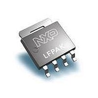
PSMN1R9-25YLC,115 NXP Semiconductors, PSMN1R9-25YLC,115 Datasheet - Page 5

PSMN1R9-25YLC,115
Manufacturer Part Number
PSMN1R9-25YLC,115
Description
MOSFET Power N-Ch 25V 2.05 mOhms
Manufacturer
NXP Semiconductors
Series
-r
Datasheet
1.PSMN1R9-25YLC115.pdf
(15 pages)
Specifications of PSMN1R9-25YLC,115
Transistor Polarity
N-Channel
Resistance Drain-source Rds (on)
2.05 mOhms
Drain-source Breakdown Voltage
25 V
Gate-source Breakdown Voltage
20 V
Continuous Drain Current
100 A
Power Dissipation
141 W
Maximum Operating Temperature
+ 175 C
Mounting Style
SMD/SMT
Package / Case
LFPAK
Gate Charge Qg
57 nC
Minimum Operating Temperature
- 55 C
Fet Type
MOSFET N-Channel, Metal Oxide
Fet Feature
Logic Level Gate
Rds On (max) @ Id, Vgs
2.05 mOhm @ 25A, 10V
Drain To Source Voltage (vdss)
25V
Current - Continuous Drain (id) @ 25° C
100A
Vgs(th) (max) @ Id
1.95V @ 1mA
Gate Charge (qg) @ Vgs
57nC @ 10V
Input Capacitance (ciss) @ Vds
3504pF @ 12V
Power - Max
141W
Mounting Type
Surface Mount
Lead Free Status / Rohs Status
Details
Other names
934065201115
NXP Semiconductors
6. Thermal characteristics
Table 6.
PSMN1R9-25YLC
Product data sheet
Symbol
R
Fig 4.
Fig 5.
th(j-mb)
Z
(K/W)
th(j-mb)
(A)
I
D
10
10
10
10
10
10
10
10
10
-1
-2
-3
-1
1
4
3
2
1
10
1e-6
Safe operating area; continuous and peak drain currents as a function of drain-source voltage
Transient thermal impedance from junction to mounting base as a function of pulse duration
-1
δ = 0.5
0.2
0.05
0.02
0.1
Thermal characteristics
single shot
Parameter
thermal resistance from
junction to mounting base
10
-5
Limit R
DSon
= V
DS
All information provided in this document is subject to legal disclaimers.
10
/ I
1
D
-4
Conditions
see
Rev. 1 — 2 May 2011
N-channel 25 V 2.05 mΩ logic level MOSFET in LFPAK using
Figure 5
DC
10
-3
10
10
-2
PSMN1R9-25YLC
Min
-
V
t
100 μ s
1 ms
10 ms
100 ms
DS
p
10
=10 μ s
P
(V)
-1
Typ
0.92
t
p
T
© NXP B.V. 2011. All rights reserved.
t
p
003aaf826
003aaf827
δ =
(s)
Max
1.06
t
T
p
t
10
1
2
Unit
K/W
5 of 15


