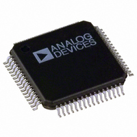
ADV7180BSTZ Analog Devices Inc, ADV7180BSTZ Datasheet - Page 22

ADV7180BSTZ
Manufacturer Part Number
ADV7180BSTZ
Description
IC VIDEO DECODER SDTV 64-LQFP
Manufacturer
Analog Devices Inc
Type
Video Decoderr
Datasheet
1.ADV7180BSTZ.pdf
(116 pages)
Specifications of ADV7180BSTZ
Design Resources
Low Cost Differential Video Receiver Using ADA4851 Amplifier and ADV7180 Video Decoder (CN0060) Low Cost Video Multiplexer for Video Switching Using ADA4853-2 Op Amp with Disable Function (CN0076)
Applications
Digital Cameras, Mobile Phones, Portable Video
Voltage - Supply, Analog
1.71 V ~ 1.89 V
Voltage - Supply, Digital
1.65 V ~ 2 V
Mounting Type
Surface Mount
Package / Case
64-LQFP
Resolution (bits)
10bit
Input Format
Analog
Output Format
Digital
Adc Sample Rate
57.27MSPS
Power Dissipation Pd
15µW
No. Of Input Channels
6
Supply Voltage Range
1.71V To 1.89V
Lead Free Status / RoHS Status
Lead free / RoHS Compliant
For Use With
EVAL-ADV7180LQEBZ - BOARD EVALUATION ADV7180EVAL-ADV7180LFEBZ - BOARD EVAL FOR ADV7180 LFCSP
Lead Free Status / RoHS Status
Lead free / RoHS Compliant, Lead free / RoHS Compliant
Available stocks
Company
Part Number
Manufacturer
Quantity
Price
Company:
Part Number:
ADV7180BSTZ
Manufacturer:
AMIS
Quantity:
6 240
Company:
Part Number:
ADV7180BSTZ
Manufacturer:
Analog Devices Inc
Quantity:
10 000
Part Number:
ADV7180BSTZ
Manufacturer:
ADI/亚德诺
Quantity:
20 000
Company:
Part Number:
ADV7180BSTZ-REEL
Manufacturer:
Analog Devices Inc
Quantity:
10 000
ADV7180
Timing Signals Output Enable
TIM_OE, Address 0x04[3]
The TIM_OE bit should be regarded as an addition to the TOD bit.
Setting it high forces the output drivers for HS, VS, and FIELD into
the active state (that is, driving state) even if the TOD bit is set.
If TIM_OE is set to low, the HS, VS, and FIELD pins are three-
stated depending on the TOD bit. This functionality is beneficial if
the decoder is only used as a timing generator. This may be the
case if only the timing signals are extracted from an incoming
signal or if the part is in free-run mode, where a separate chip
can output a company logo, for example.
For more information on three-state control, see the Three-
State Output Drivers section and the Three-State LLC Driver
section.
Individual drive strength controls are provided via the
DR_STR_x bits.
When TIM_OE is 0 (default), HS, VS, and FIELD are three-
stated according to the TOD bit.
When TIM_OE is 1, HS, VS, and FIELD are forced active all
the time.
Drive Strength Selection (Data)
DR_STR[1:0], Address 0xF4[5:4]
For EMC and crosstalk reasons, it may be desirable to strengthen or
weaken the drive strength of the output drivers. The DR_STR[1:0]
bits affect the P[15:0] for the 64-lead device or P[7:0] for the
48-lead, 40-lead, and 32-lead devices output drivers.
For more information on three-state control, see the Drive
Strength Selection (Clock) and the Drive Strength Selection
(Sync) sections.
Table 16. DR_STR Function
DR_STR[1:0]
00
01 (default)
10
11
Drive Strength Selection (Clock)
DR_STR_C[1:0], Address 0xF4[3:2]
The DR_STR_C[1:0] bits can be used to select the strength of
the clock signal output driver (LLC pin). For more information,
see the Drive Strength Selection (Sync) and the Drive Strength
Selection (Data) sections.
Low drive strength (1×)
Medium low drive strength (2×)
Medium high drive strength (3×)
High drive strength (4×)
Description
Rev. F | Page 22 of 116
Table 17. DR_STR_C Function
DR_STR_C[1:0]
00
01 (default)
10
11
Drive Strength Selection (Sync)
DR_STR_S[1:0], Address 0xF4[1:0]
The DR_STR_S[1:0] bits allow the user to select the strength of
the synchronization signals with which HS, VS, and FIELD are
driven. For more information, see the Drive Strength Selection
(Data) section.
Table 18. DR_STR_S Function
DR_STR_S[1:0]
00
01 (default)
10
11
Enable Subcarrier Frequency Lock Pin
EN_SFL_PIN, Address 0x04[1]
The EN_SFL_PIN bit enables the output of subcarrier lock
information (also known as genlock) from the ADV7180 core
to an encoder in a decoder/encoder back-to-back arrangement.
When EN_SFL_PIN is 0 (default), the subcarrier frequency lock
output is disabled.
When EN_SFL_PIN is 1, the subcarrier frequency lock information
is presented on the SFL pin.
Polarity LLC Pin
PCLK, Address 0x37[0]
The polarity of the clock that leaves the ADV7180 via the LLC
pin can be inverted using the PCLK bit.
Changing the polarity of the LLC clock output may be necessary to
meet the setup-and-hold time expectations of follow-on chips.
When PCLK is 0, the LLC output polarity is inverted.
When PCLK is 1 (default), the LLC output polarity is normal
(see the Timing Specifications section).
Description
Low drive strength (1×)
Medium low drive strength (2×)
Medium high drive strength (3×)
High drive strength (4×)
Description
Low drive strength (1×)
Medium low drive strength (2×)
Medium high drive strength (3×)
High drive strength (4×)


