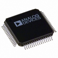
ADV7180BSTZ Analog Devices Inc, ADV7180BSTZ Datasheet - Page 64

ADV7180BSTZ
Manufacturer Part Number
ADV7180BSTZ
Description
IC VIDEO DECODER SDTV 64-LQFP
Manufacturer
Analog Devices Inc
Type
Video Decoderr
Datasheet
1.ADV7180BSTZ.pdf
(116 pages)
Specifications of ADV7180BSTZ
Design Resources
Low Cost Differential Video Receiver Using ADA4851 Amplifier and ADV7180 Video Decoder (CN0060) Low Cost Video Multiplexer for Video Switching Using ADA4853-2 Op Amp with Disable Function (CN0076)
Applications
Digital Cameras, Mobile Phones, Portable Video
Voltage - Supply, Analog
1.71 V ~ 1.89 V
Voltage - Supply, Digital
1.65 V ~ 2 V
Mounting Type
Surface Mount
Package / Case
64-LQFP
Resolution (bits)
10bit
Input Format
Analog
Output Format
Digital
Adc Sample Rate
57.27MSPS
Power Dissipation Pd
15µW
No. Of Input Channels
6
Supply Voltage Range
1.71V To 1.89V
Lead Free Status / RoHS Status
Lead free / RoHS Compliant
For Use With
EVAL-ADV7180LQEBZ - BOARD EVALUATION ADV7180EVAL-ADV7180LFEBZ - BOARD EVAL FOR ADV7180 LFCSP
Lead Free Status / RoHS Status
Lead free / RoHS Compliant, Lead free / RoHS Compliant
Available stocks
Company
Part Number
Manufacturer
Quantity
Price
Company:
Part Number:
ADV7180BSTZ
Manufacturer:
AMIS
Quantity:
6 240
Company:
Part Number:
ADV7180BSTZ
Manufacturer:
Analog Devices Inc
Quantity:
10 000
Part Number:
ADV7180BSTZ
Manufacturer:
ADI/亚德诺
Quantity:
20 000
Company:
Part Number:
ADV7180BSTZ-REEL
Manufacturer:
Analog Devices Inc
Quantity:
10 000
ADV7180
VITC
VITC has a sequence of 10 syncs between each data byte. The
VDP strips these syncs from the data stream to output only the
data bytes. The VITC results are available in Register
VDP_VITC_DATA_0 to Register VDP_VITC_DATA_8
(Register 0x92 to Register 0x9A, user sub map).
The VITC has a CRC byte at the end; the syncs in between each
data byte are also used in this CRC calculation. Because the syncs
in between each data byte are not output, the CRC is calculated
internally. The calculated CRC is available for the user in the
VDP_VITC_CALC_CRC register (Resister 0x9B, user sub map).
When the VDP completes decoding the VITC line, the
VITC_DATA_x and VITC_CRC registers are updated and the
VITC_AVL bit is set.
Table 83. VITC Readback Registers
Signal Name
VITC_DATA_0[7:0]
VITC_DATA_1[7:0]
VITC_DATA_2[7:0]
VITC_DATA_3[7:0]
VITC_DATA_4[7:0]
VITC_DATA_5[7:0]
VITC_DATA_6[7:0]
VITC_DATA_7[7:0]
VITC_DATA_8[7:0]
VITC_CRC[7:0]
1
These registers are readback registers; default value does not apply.
BIT 0, BIT 1
1
Figure 49. VITC Waveform and Decoded Data Correlation
Rev. F | Page 64 of 116
VDP_VITC_DATA_1[7:0] (VITC Bits[19:12])
VDP_VITC_DATA_2[7:0] (VITC Bits[29:22])
VDP_VITC_DATA_3[7:0] (VITC Bits[39:32])
VDP_VITC_DATA_4[7:0] (VITC Bits[49:42])
VDP_VITC_DATA_5[7:0] (VITC Bits[59:52])
VDP_VITC_DATA_6[7:0] (VITC Bits[69:62])
VDP_VITC_DATA_7[7:0] (VITC Bits[79:72])
VDP_VITC_DATA_8[7:0] (VITC Bits[89:82])
Register Location
VDP_VITC_DATA_0[7:0] (VITC Bits[9:2])
VDP_VITC_CALC_CRC[7:0]
VITC WAVEFORM
TO
VITC_CLEAR, VITC Clear, Address 0x78[6],
User Sub Map, Write Only, Self-Clearing
Setting VITC_CLEAR to 1 reinitializes the VITC readback
registers.
VITC_AVL, VITC Available, Address 0x78[6],
User Sub Map, Read Only
When VITC_AVL is 0, VITC data was not detected.
When VITC_AVL is 1, VITC data was detected.
VITC Readback Registers
See Figure 49 for the I
2
C-to-VITC bit mapping.
BIT 88, BIT 89
146
147
148
149
150
151
152
153
154
155
Address (User Sub Map)
0x92
0x93
0x94
0x95
0x96
0x97
0x98
0x99
0x9A
0x9B


