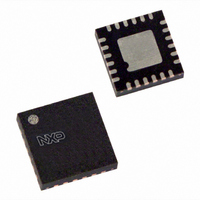
PCA9502BS,151 NXP Semiconductors, PCA9502BS,151 Datasheet - Page 5

PCA9502BS,151
Manufacturer Part Number
PCA9502BS,151
Description
IC I/O EXPANDER I2C/SPI 24HVQFN
Manufacturer
NXP Semiconductors
Datasheet
1.PCA9502BS151.pdf
(25 pages)
Specifications of PCA9502BS,151
Package / Case
24-VQFN Exposed Pad, 24-HVQFN, 24-SQFN, 24-DHVQFN
Interface
I²C, SPI
Number Of I /o
8
Interrupt Output
No
Frequency - Clock
400kHz
Voltage - Supply
2.3 V ~ 3.6 V
Operating Temperature
-40°C ~ 85°C
Mounting Type
Surface Mount
Logic Family
PCA
Number Of Lines (input / Output)
14 / 11
Operating Supply Voltage
3.3 V / 2.5 V
Power Dissipation
300 mW
Operating Temperature Range
- 40 C to + 85 C
Logic Type
I/O Expander
Mounting Style
SMD/SMT
Number Of Input Lines
14
Number Of Output Lines
11
Output Current
+/- 10 mA
Output Voltage
2.4 V
Lead Free Status / RoHS Status
Lead free / RoHS Compliant
Lead Free Status / RoHS Status
Lead free / RoHS Compliant, Lead free / RoHS Compliant
Other names
568-3635
935281363151
PCA9502BS-S
935281363151
PCA9502BS-S
NXP Semiconductors
8. Register descriptions
Table 6.
[1]
[2]
PCA9502_3
Product data sheet
Register
address
General Register Set
0x0A
0x0B
0x0C
0x0D
0x0E
Other addresses 0x00 through 0x09, 0x0F are reserved and should not be accessed (read or write).
These bits are reserved and should be set to 0.
[1]
[1]
[1]
[1]
[1]
Register
IODir
IOState
IOIntEna
reserved
[2]
IOControl reserved
PCA9502 internal registers
7.2 Interrupts
8.1 Programmable I/O pins Direction register (IODir)
Bit 7
bit 7
bit 7
bit 7
reserved
[2]
[2]
The PCA9502 has interrupt generation capability. The interrupt enable register (IOIntEna)
enables interrupts due to I/O pin change of state, and the IRQ signal in response to an
interrupt generation.
The programming combinations for register selection are shown in
Table 5.
This register is used to program the I/O pins direction. Bit 0 to bit 7 control GPIO0 to
GPIO7.
Table 7.
Remark: If there is a pending input (GPIO) interrupt and IODir is written, this pending
interrupt will be cleared, that is, the interrupt signal will be negated.
Register name
IODir
IOState
IOIntEna
IOControl
Bit
7:0
Bit 6
bit 6
bit 6
bit 6
reserved
[2]
reserved
[2]
Symbol
IODir
Register map - read/write properties
IODir register (address 0x0A) bit description
Read mode
I/O pin direction
I/O pin states
I/O interrupt enable register
I/O pins control
Bit 5
bit 5
bit 5
bit 5
reserved
[2]
reserved
[2]
Rev. 03 — 13 October 2006
Description
set GPIO pins 7:0 to input or output
0 = input
1 = output
Bit 4
bit 4
bit 4
bit 4
reserved
[2]
reserved
[2]
Bit 3
bit 3
bit 3
bit 3
reserved
[2]
SReset
8-bit I/O expander with I
Bit 2
bit 2
bit 2
bit 2
reserved
[2]
reserved
[2]
Write mode
I/O pin direction
n/a
I/O interrupt enable register
I/O pins control
Bit 1
bit 1
bit 1
bit 1
reserved
[2]
reserved
[2]
Table
2
C-bus/SPI interface
PCA9502
© NXP B.V. 2006. All rights reserved.
5.
Bit 0
bit 0
bit 0
bit 0
reserved
[2]
IOLatch
5 of 25
R/W
R/W
R/W
R/W
R/W


