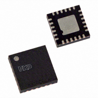
PCA9502BS,151 NXP Semiconductors, PCA9502BS,151 Datasheet - Page 8

PCA9502BS,151
Manufacturer Part Number
PCA9502BS,151
Description
IC I/O EXPANDER I2C/SPI 24HVQFN
Manufacturer
NXP Semiconductors
Datasheet
1.PCA9502BS151.pdf
(25 pages)
Specifications of PCA9502BS,151
Package / Case
24-VQFN Exposed Pad, 24-HVQFN, 24-SQFN, 24-DHVQFN
Interface
I²C, SPI
Number Of I /o
8
Interrupt Output
No
Frequency - Clock
400kHz
Voltage - Supply
2.3 V ~ 3.6 V
Operating Temperature
-40°C ~ 85°C
Mounting Type
Surface Mount
Logic Family
PCA
Number Of Lines (input / Output)
14 / 11
Operating Supply Voltage
3.3 V / 2.5 V
Power Dissipation
300 mW
Operating Temperature Range
- 40 C to + 85 C
Logic Type
I/O Expander
Mounting Style
SMD/SMT
Number Of Input Lines
14
Number Of Output Lines
11
Output Current
+/- 10 mA
Output Voltage
2.4 V
Lead Free Status / RoHS Status
Lead free / RoHS Compliant
Lead Free Status / RoHS Status
Lead free / RoHS Compliant, Lead free / RoHS Compliant
Other names
568-3635
935281363151
PCA9502BS-S
935281363151
PCA9502BS-S
NXP Semiconductors
PCA9502_3
Product data sheet
Fig 6. Data transfer on the I
Fig 7. Acknowledge on the I
SDA
SCL
condition
SCL from master
START
by transmitter
S
data output
data output
by receiver
9.2 Addressing and transfer formats
MSB
A slave receiver must generate an acknowledge after the reception of each byte, and a
master must generate one after the reception of each byte clocked out of the slave
transmitter.
There is an exception to the ‘acknowledge after every byte’ rule. It occurs when a master
is a receiver: it must signal an end of data to the transmitter by not signalling an
acknowledge on the last byte that has been clocked out of the slave. The acknowledge
related clock, generated by the master should still take place, but the SDA line will not be
pulled down. In order to indicate that this is an active and intentional lack of
acknowledgement, we shall term this special condition as a ‘negative acknowledge’.
Each device on the bus has its own unique address. Before any data is transmitted on the
bus, the master transmits on the bus the address of the slave to be accessed for this
transaction. A well-behaved slave with a matching address, if it exists on the network,
should of course acknowledge the master's addressing. The addressing is done by the
first byte transmitted by the master after the START condition.
An address on the network is seven bits long, appearing as the most significant bits of the
address byte. The last bit is a direction (R/W) bit. A ‘0’ indicates that the master is
transmitting (write) and a ‘1’ indicates that the master requests data (read). A complete
data transfer, comprised of an address byte indicating a ‘write’ and two data bytes is
shown in
0
condition
START
2
2
S
C-bus
1
C-bus
Figure
interrupt within receiver
8.
0
6
byte complete,
Rev. 03 — 13 October 2006
1
7
ACK
8
acknowledgement signal
from receiver
6
7
0
8-bit I/O expander with I
clock line held LOW
while interrupt is serviced
8
1
002aab013
2 to 7
transmitter stays off of the bus
during the acknowledge clock
acknowledgement signal
from receiver
ACK
8
2
C-bus/SPI interface
PCA9502
© NXP B.V. 2006. All rights reserved.
condition
STOP
P
002aab012
8 of 25


