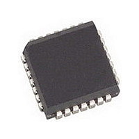
AMIS49587C5871RG ON Semiconductor, AMIS49587C5871RG Datasheet - Page 14

AMIS49587C5871RG
Manufacturer Part Number
AMIS49587C5871RG
Description
IC MODEM PLC 50/60MHZ 28PLCC
Manufacturer
ON Semiconductor
Specifications of AMIS49587C5871RG
Baud Rates
Selectable
Interface
SCI
Voltage - Supply
3 V ~ 3.6 V
Mounting Type
Surface Mount
Package / Case
28-PLCC
Number Of Transmitters
1
Power Supply Requirement
Single
Package Type
PLCC
Operating Temperature Classification
Commercial
Mounting
Surface Mount
Pin Count
28
Operating Temperature (max)
70C
Dual Supply Voltage (typ)
Not RequiredV
Dual Supply Voltage (max)
Not RequiredV
Dual Supply Voltage (min)
Not RequiredV
Lead Free Status / RoHS Status
Lead free / RoHS Compliant
Data Format
-
Lead Free Status / Rohs Status
Compliant
Available stocks
Company
Part Number
Manufacturer
Quantity
Price
Company:
Part Number:
AMIS49587C5871RG
Manufacturer:
ON
Quantity:
3 400
Company:
Part Number:
AMIS49587C5871RG
Manufacturer:
ON Semiconductor
Quantity:
10 000
The space and mark frequency can be calculated as:
•
•
Or the content of both R_FS[15:0] and R_FM[15:0] are
defined as:
•
•
(when TX_RXB goes from 0 to 1) the phase accumulator
DA Converter
digital word to a pulse density modulated (PDM) signal. The
PDM signal is converted to an analog signal with a first order
switched capacitor filter.
Low Pass Filter
path filters the quantization noise and noise generated by the
SD DA converter. The low pass filter has a circuit which
tunes the RC time constants of the filter towards the process
characteristics. The C values for the LPF filter are controlled
by the ARM micro controller.
Table 22. SPACE AND MARK FREQUENCY
SELECTION
R_FM[15:0]
R_FS[15:0]
After a hard or soft reset or at the start of the transmission
A digital to analog SD converter converts the sine wave
A 3
f
f
R_FS[15:0]_dec = Round(2
R_FM[15:0]_dec = Round(2
♦
S
M
Register
ARM
= R_FS[15:0]_dec x f
synthesizer clock frequency.
= R_FM[15:0]_dec x f
Where f
rd
order continuous time low pass filter in the transmit
TX_DATA
BIT_CLK
TX_RXB
TX_ENB
TX_OUT
DDS
(See Appendix C)
Reset
0000h
0000h
= 3 MHz is the direct digital
Step register for the space
frequency f
Step register for the mark
frequency f
DDS
DDS
18
/2
18
/2
18
x f
x f
18
S
Description
S
M
M
/f
DDS
/f
DDS
)
)
Figure 7. TX_ENB Timing
http://onsemi.com
14
must start at it’s 0 phase position, corresponding with a 0 V
output level. When switching between f
accumulator must give a continuous phase and not restart
from phase 0.
TX_RXB goes from 1 to 0) the sine wave generator must
make sure to complete the active sine period.
TX_ENB to enable the external power amplifier. TX_ENB
is 1 when the AMIS−49587 is in receive mode. TX_ENB is
0 when AMIS−49587 is in transmit mode. When going from
transmit to receive mode (TX_RXB goes from 1 to 0) the
TX_ENB signal is kept active for a short period of t
TX_DATA which corresponds to the transmitted SFSK
signal. When transmitting f
transmitting f
is not enabled (TX_RXB = 0) TX_DATA goes to logic 1 at
the next BIT_CLK.
Amplifier with Automatic Level Control (ALC)
transmitter output level. First a peak detection is done. The
peak value is compared to 2 thresholds levels: VTL
and VTH
control the setting of the level of TX_OUT. The level of
TX_OUT can be attenuated in 8 steps of 3 dB typical.
(maximum attenuation) When going to reception mode
(when TX_RXB goes from 1 to 0) the level is kept in
memory so that the next transmit frame starts with the old
When AMIS−49587 goes into receive mode (when
The control logic for the transmitter generates a signal
The control logic for the transmitter generates a signal
The pin ALC_IN is used for level control of the
After hard or soft reset the level is set at minimum level
ALC_IN
S
t
dTX_ENB
TX_DATA is logic 0. When the transmitter
. The result of the peak detection is used to
M
TX_DATA is logic 1. When
M
and f
S
the phase
dTX_ENB
ALC_IN
.


