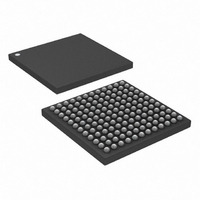
DS33X11+ Maxim Integrated Products, DS33X11+ Datasheet - Page 19

DS33X11+
Manufacturer Part Number
DS33X11+
Description
IC MAPPING ETHERNET 144CSBGA
Manufacturer
Maxim Integrated Products
Datasheet
1.DS33X11.pdf
(375 pages)
Specifications of DS33X11+
Applications
Data Transport
Interface
SPI
Voltage - Supply
1.8V, 2.5V, 3.3V
Package / Case
144-CSBGA
Mounting Type
Surface Mount
Lead Free Status / RoHS Status
Lead free / RoHS Compliant
- Current page: 19 of 375
- Download datasheet (3Mb)
5.3
All devices in the product family require an external DDR SDRAM for operation. The user must select a JEDEC
JESD79D compliant DDR SDRAM. DDR 266 or faster may be used. The recommended size is 256 Mbit (4 Meg x
16 x 4 banks), although it is possible to use other sizes (see Section 5.4). P2P operation is supported, and 0-ohm
series termination is possible with proper PCB layout.
All devices in the product family require an external microprocessor for configuration and status monitoring.
Because the DS33X162 family of devices are designed to require only a minimal amount of processor support, an
inexpensive microcontroller can normally be used. In applications which make extensive use of the support for
higher-layer protocols may require additional protocol processing capability, microprocessor selection can normally
be determined by evaluating the management frame processing requirements of the particular application. All
devices in the product family are designed to support both polled and interrupt-driven environments.
Microprocessor control is possible through the 8-bit parallel control port or SPI Slave port. More information on
microprocessor control is available in Section 8.1. Note that the parallel bus is not available in the 144 pin
DS33X11, and the SPI Slave port must be used for processor control.
Depending on the application, external PDH framers and LIUs may be required. Maxim offers a broad range of
framers, LIUs, and single-chip transceivers compatible with the DS33X162 family of products.
The Ethernet interface will normally be connected to an external Ethernet PHY or Ethernet switch device. Many
commercially-available products are available and will seamlessly interface with the device’s MII, RMII, or GMII
options.
Several external clock sources are required for proper operation. See Section 8.3 for more information.
5.4
Note that all devices except the DS33X11, DS33W11, and DS33W41 share a common footprint. This is intended to
make it very easy to design a circuit that easily scales from 4 to 16 WAN ports with alternate assembly BOMs.
When designing a PCB for 4 or 8 ports, care should be taken to tie the unused input pins for serial ports 5-16 or 9-
16 to ground. This will allow for use of the higher density device for prototype purposes. Care should be taken that
outputs from the DS33X162 family device that are present in the high-port count option but not in the low port-count
option may potentially leave inputs on other devices floating, and should be pulled appropriately to a known
voltage.
The device’s DDR SDRAM interface is designed to use a JESD79D 256 Mbit (4 Meg x 16 x 4 bank) DDR SDRAM
with a 16 bit data bus. If a larger DDR SDRAM must be used, the lowest 13 address lines (A0-A12) should be
used, and care should be taken to ground any unused address inputs on the DDR SDRAM. Note that in such a
case, only 256 Mbits are addressable by the device. If a smaller JESD79D DDR SDRAM is to be used (such as the
128 Mbit MT46V8M16), the unused address outputs should be left unconnected, and care should be taken in
software to keep the starting and ending addresses of each queue within the same memory bank. In all cases, P2P
operation is supported, and 0Ω series termination is possible with proper PCB layout.
5.5
The DDR SDRAM interface has particularly stringent layout requirements. Traces should have matched
impedances, be of equal length, and should not have stubs. Refer to the DDR SDRAM’s data sheet for more
information. Supply decoupling should be placed as close to the device as possible.
5.6
All devices in the product family have a common register set. An example initialization sequence is shown in
Section 8.5. Software drivers and demonstration kit software are both available from Maxim. Go to
www.maxim-ic.com/support
Rev: 063008
________________________________________________ DS33X162/X161/X82/X81/X42/X41/X11/W41/W11
Ancillary Device Selection
Circuit Design
Board Layout
Software Development
for the latest information.
19 of 375
Related parts for DS33X11+
Image
Part Number
Description
Manufacturer
Datasheet
Request
R

Part Number:
Description:
MAX7528KCWPMaxim Integrated Products [CMOS Dual 8-Bit Buffered Multiplying DACs]
Manufacturer:
Maxim Integrated Products
Datasheet:

Part Number:
Description:
Single +5V, fully integrated, 1.25Gbps laser diode driver.
Manufacturer:
Maxim Integrated Products
Datasheet:

Part Number:
Description:
Single +5V, fully integrated, 155Mbps laser diode driver.
Manufacturer:
Maxim Integrated Products
Datasheet:

Part Number:
Description:
VRD11/VRD10, K8 Rev F 2/3/4-Phase PWM Controllers with Integrated Dual MOSFET Drivers
Manufacturer:
Maxim Integrated Products
Datasheet:

Part Number:
Description:
Highly Integrated Level 2 SMBus Battery Chargers
Manufacturer:
Maxim Integrated Products
Datasheet:

Part Number:
Description:
Current Monitor and Accumulator with Integrated Sense Resistor; ; Temperature Range: -40°C to +85°C
Manufacturer:
Maxim Integrated Products

Part Number:
Description:
TSSOP 14/A�/RS-485 Transceivers with Integrated 100O/120O Termination Resis
Manufacturer:
Maxim Integrated Products

Part Number:
Description:
TSSOP 14/A�/RS-485 Transceivers with Integrated 100O/120O Termination Resis
Manufacturer:
Maxim Integrated Products

Part Number:
Description:
QFN 16/A�/AC-DC and DC-DC Peak-Current-Mode Converters with Integrated Step
Manufacturer:
Maxim Integrated Products

Part Number:
Description:
TDFN/A/65V, 1A, 600KHZ, SYNCHRONOUS STEP-DOWN REGULATOR WITH INTEGRATED SWI
Manufacturer:
Maxim Integrated Products

Part Number:
Description:
Integrated Temperature Controller f
Manufacturer:
Maxim Integrated Products

Part Number:
Description:
SOT23-6/I�/45MHz to 650MHz, Integrated IF VCOs with Differential Output
Manufacturer:
Maxim Integrated Products

Part Number:
Description:
SOT23-6/I�/45MHz to 650MHz, Integrated IF VCOs with Differential Output
Manufacturer:
Maxim Integrated Products

Part Number:
Description:
EVALUATION KIT/2.4GHZ TO 2.5GHZ 802.11G/B RF TRANSCEIVER WITH INTEGRATED PA
Manufacturer:
Maxim Integrated Products

Part Number:
Description:
QFN/E/DUAL PCIE/SATA HIGH SPEED SWITCH WITH INTEGRATED BIAS RESISTOR
Manufacturer:
Maxim Integrated Products
Datasheet:


