DS33X11+ Maxim Integrated Products, DS33X11+ Datasheet - Page 330
DS33X11+
Manufacturer Part Number
DS33X11+
Description
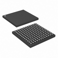
IC MAPPING ETHERNET 144CSBGA
Manufacturer
Maxim Integrated Products
Datasheet
1.DS33X11.pdf
(375 pages)
Specifications of DS33X11+
Applications
Data Transport
Interface
SPI
Voltage - Supply
1.8V, 2.5V, 3.3V
Package / Case
144-CSBGA
Mounting Type
Surface Mount
Lead Free Status / RoHS Status
Lead free / RoHS Compliant


SPI_MOSI
SPI_MISO
SPI_MOSI
SPI_MISO
SPI_CLK
SPI_CLK
11.
11.1 Functional SPI Interface Timing
Note: The transmit and receive order of the address and data bits are selected by the SPI_SWAP pin. The R/W
(read/write) MSB bit and B (burst) LSB bit position is not affected by the SPI_SWAP pin setting.
11.1.1 SPI Transmission Format and CPHA Polarity
When SPI_CPHA = 0, CS may be de-asserted between accesses. An access is defined as one or two control
bytes followed by a data byte. CS cannot be de-asserted between the control bytes, or between the last control
byte and the data byte. When SPI_CPHA = 0, CS may also remain asserted between accesses. If it remains
asserted and the BURST bit is set, no additional control bytes are expected after the first control byte(s) and data
are transferred. If the BURST bit is set, the address will be incremented for each additional byte of data transferred
until CS is de-asserted. If CS remains asserted and the BURST bit is not set, a control byte(s) is expected following
the data byte, and the address for the next access will be received from that. Anytime CS is de-asserted, the
BURST access is terminated.
When SPI_CPHA = 1, CS may remain asserted for more than one access without being toggled high and then low
again between accesses. If the BURST bit is set, the address should increment and no additional control bytes are
expected. If the BURST bit is not set, each data byte will be followed by the control byte(s) for the next access.
Additionally, CS may also be de-asserted between accesses when SPI_CPHA =1. In the case, any BURST access
is terminated, and the next byte received when CS is re-asserted will be a control byte.
The following diagrams describe the functionality of the SPI port for the four combinations of SPI_CPOL and
SPI_CPHA. They indicate the clock edge that samples the data and the level of the clock during no-transfer events
(high or low). Since the SPI port acts as a slave device, the master device provides the clock. The user must
configure the SPI_CPOL and SPI_CPHA pins to describe which type of clock that the master device is providing.
Note that due to the address space of the device, the unused bits A13, A12, and A11 should always be zero.
Figure 11-1. SPI Serial Port Access For Read Mode, SPI_CPOL=0, SPI_CPHA = 0
Figure 11-2. SPI Serial Port Access For Read Mode, SPI_CPOL = 1, SPI_CPHA = 0
Rev: 063008
MOSI
MISO
MOSI
MISO
________________________________________________ DS33X162/X161/X82/X81/X42/X41/X11/W41/W11
SCK
SCK
CS*
CS*
CS
CS
Functional Timing
MSB
MSB
1
1
A13
A13
A12
A12
A11
A11
A10
A10
A9
A9
A8
A8
LSB
LSB
A7
A7
MSB
MSB
A6
A6
A5
A5
A4
A4
A3
A3
A2
A2
A1
A1
A0
A0
LSB
LSB
B
B
MSB
MSB
D7
D7
D6
D6
D5
D5
D4
D4
D3
D3
D2
D2
D1
D1
330 of 375
LSB
LSB
D0
D0
Related parts for DS33X11+
Image
Part Number
Description
Manufacturer
Datasheet
Request
R

Part Number:
Description:
MAX7528KCWPMaxim Integrated Products [CMOS Dual 8-Bit Buffered Multiplying DACs]
Manufacturer:
Maxim Integrated Products
Datasheet:
Part Number:
Description:
Single +5V, fully integrated, 1.25Gbps laser diode driver.
Manufacturer:
Maxim Integrated Products
Datasheet:
Part Number:
Description:
Single +5V, fully integrated, 155Mbps laser diode driver.
Manufacturer:
Maxim Integrated Products
Datasheet:
Part Number:
Description:
VRD11/VRD10, K8 Rev F 2/3/4-Phase PWM Controllers with Integrated Dual MOSFET Drivers
Manufacturer:
Maxim Integrated Products
Datasheet:
Part Number:
Description:
Highly Integrated Level 2 SMBus Battery Chargers
Manufacturer:
Maxim Integrated Products
Datasheet:
Part Number:
Description:
Current Monitor and Accumulator with Integrated Sense Resistor; ; Temperature Range: -40°C to +85°C
Manufacturer:
Maxim Integrated Products
Part Number:
Description:
TSSOP 14/A�/RS-485 Transceivers with Integrated 100O/120O Termination Resis
Manufacturer:
Maxim Integrated Products
Part Number:
Description:
TSSOP 14/A�/RS-485 Transceivers with Integrated 100O/120O Termination Resis
Manufacturer:
Maxim Integrated Products
Part Number:
Description:
QFN 16/A�/AC-DC and DC-DC Peak-Current-Mode Converters with Integrated Step
Manufacturer:
Maxim Integrated Products
Part Number:
Description:
TDFN/A/65V, 1A, 600KHZ, SYNCHRONOUS STEP-DOWN REGULATOR WITH INTEGRATED SWI
Manufacturer:
Maxim Integrated Products
Part Number:
Description:
Integrated Temperature Controller f
Manufacturer:
Maxim Integrated Products
Part Number:
Description:
SOT23-6/I�/45MHz to 650MHz, Integrated IF VCOs with Differential Output
Manufacturer:
Maxim Integrated Products
Part Number:
Description:
SOT23-6/I�/45MHz to 650MHz, Integrated IF VCOs with Differential Output
Manufacturer:
Maxim Integrated Products
Part Number:
Description:
EVALUATION KIT/2.4GHZ TO 2.5GHZ 802.11G/B RF TRANSCEIVER WITH INTEGRATED PA
Manufacturer:
Maxim Integrated Products
Part Number:
Description:
QFN/E/DUAL PCIE/SATA HIGH SPEED SWITCH WITH INTEGRATED BIAS RESISTOR
Manufacturer:
Maxim Integrated Products
Datasheet: