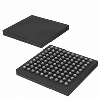
DS33ZH11+ Maxim Integrated Products, DS33ZH11+ Datasheet - Page 29

DS33ZH11+
Manufacturer Part Number
DS33ZH11+
Description
IC MAPPER ETHERNET 100CSBGA
Manufacturer
Maxim Integrated Products
Datasheet
1.DS33Z11.pdf
(172 pages)
Specifications of DS33ZH11+
Applications
Data Transport
Interface
Serial
Voltage - Supply
1.8V, 2.5V, 3.3V
Package / Case
100-LBGA
Mounting Type
Surface Mount
Lead Free Status / RoHS Status
Lead free / RoHS Compliant
- Current page: 29 of 172
- Download datasheet (2Mb)
DS33Z11 Ethernet Mapper
8
FUNCTIONAL DESCRIPTION
The DS33Z11 provides interconnection and mapping functionality between Ethernet Packet Systems and WAN
Time-Division Multiplexed (TDM) systems such as T1/E1/J1, HDSL, and T3/E3. The device is composed of a
10/100 Ethernet MAC, Packet Arbiter, Committed Information Rate controller (CIR), HDLC/X.86(LAPS) Mapper,
SDRAM interface, control ports, and Bit Error Rate Tester (BERT).
The Ethernet Packet interface supports MII and RMII interfaces allowing DSZ33Z11 to connect to commercially
available Ethernet PHY and MAC devices. The Ethernet interface can be configured for 10 Mbps or 100 Mbps
service, in DTE and DCE configurations. The DS33Z11 MAC interface rejects frames with bad FCS and short
frames (less than 64 bytes).
Ethernet frames are queued and stored in external 32-bit SDRAM. The DS33Z11 SDRAM controller enables
connection to a 128Mbit SDRAM without external glue logic, at clock frequencies up to 100 MHz. The SDRAM is
used for both the Transmit and Receive Data Queues. The Receive Queue stores data to be sent from the Packet
interface to the WAN interface. The Transmit Queue stores data to be sent from the WAN interface to the Packet
interface. The external SDRAM can accommodate up to 8192 frames with a maximum frame size of 2016 bytes.
The sizing of the queues can be adjusted by software. The user can also program high and low watermarks for
each queue that can be used for automatic or manual flow control. The packet data stored in the SDRAM is
encapsulated in HDLC or X.86 (LAPS) to be transmitted over the WAN interface. The device also provides the
capability for bit and packet scrambling.
The WAN interface also receives encapsulated Ethernet packets and transmits the extracted packets over the
Ethernet port. The WAN physical interface supports serial data streams up to 52 Mbps. The WAN serial port can
operate with a gapped clock, and can be connected to a framer, electrical LIU, optical transceiver, or T/E-Carrier
transceiver for transmission to the WAN. The WAN interface can be connected to the Dallas
Semiconductor/Maxim T1/E1/J1 framers, LIUs, and SCTs. The WAN interface can also be connected to the
Dallas Semiconductor/Maxim T3/E3/STS-1 framers, LIUs, and SCTs to provide T3, E3, and STS1 connectivity.
The DS33Z11 can be configured through an 8-bit microprocessor interface port. A serial EEPROM (SPI) interface
and hardware mode are also included for applications without a host microprocessor. Operation without an
external host simplifies and reduces the cost of typical applications such as connectivity to T1/T3 and E1/E3 front
ends. The DS33Z11 also provides two on-board clock dividers for the System Clock input and Reference Clock
Input for the 802.3 interfaces, further reducing the need for ancillary devices.
8.1 Processor Interface
Microprocessor control of the DS33Z11 is accomplished through the 20 interface pins of the microprocessor port.
The 8-bit parallel data bus can be configured for Intel or Motorola modes of operation with the two MODEC[1:0]
pins. When MODEC[1:0] = 00 and HWMODE = 0, bus timing is in Intel mode, as shown in
Figure 11-9
and
Figure
11-10. When MODEC[1:0] = 01 and HWMODE = 0, bus timing is in Motorola mode, as shown in
Figure
11-11
and
Figure
11-12. The address space is mapped through the use of 8 address lines, A0-A7. Multiplexed
Mode is not supported on the processor interface.
The Chip Select (CS) pin must be brought to a logic low level to gain read and write access to the microprocessor
port. With Intel timing selected, the Read (RD) and Write (WR) pins are used to indicate read and write operations
and latch data through the interface. With Motorola timing selected, the Read-Write (RW) pin is used to indicate
read and write operations while the Data Strobe (DS) pin is used to latch data through the interface.
The interrupt output pin (INT) is an open-drain output that will assert a logic-low level upon a number of software
maskable interrupt conditions. This pin is normally connected to the microprocessor interrupt input. The register
map is shown in
Table
9-1.
29 of 172
Related parts for DS33ZH11+
Image
Part Number
Description
Manufacturer
Datasheet
Request
R

Part Number:
Description:
MAX7528KCWPMaxim Integrated Products [CMOS Dual 8-Bit Buffered Multiplying DACs]
Manufacturer:
Maxim Integrated Products
Datasheet:

Part Number:
Description:
Single +5V, fully integrated, 1.25Gbps laser diode driver.
Manufacturer:
Maxim Integrated Products
Datasheet:

Part Number:
Description:
Single +5V, fully integrated, 155Mbps laser diode driver.
Manufacturer:
Maxim Integrated Products
Datasheet:

Part Number:
Description:
VRD11/VRD10, K8 Rev F 2/3/4-Phase PWM Controllers with Integrated Dual MOSFET Drivers
Manufacturer:
Maxim Integrated Products
Datasheet:

Part Number:
Description:
Highly Integrated Level 2 SMBus Battery Chargers
Manufacturer:
Maxim Integrated Products
Datasheet:

Part Number:
Description:
Current Monitor and Accumulator with Integrated Sense Resistor; ; Temperature Range: -40°C to +85°C
Manufacturer:
Maxim Integrated Products

Part Number:
Description:
TSSOP 14/A�/RS-485 Transceivers with Integrated 100O/120O Termination Resis
Manufacturer:
Maxim Integrated Products

Part Number:
Description:
TSSOP 14/A�/RS-485 Transceivers with Integrated 100O/120O Termination Resis
Manufacturer:
Maxim Integrated Products

Part Number:
Description:
QFN 16/A�/AC-DC and DC-DC Peak-Current-Mode Converters with Integrated Step
Manufacturer:
Maxim Integrated Products

Part Number:
Description:
TDFN/A/65V, 1A, 600KHZ, SYNCHRONOUS STEP-DOWN REGULATOR WITH INTEGRATED SWI
Manufacturer:
Maxim Integrated Products

Part Number:
Description:
Integrated Temperature Controller f
Manufacturer:
Maxim Integrated Products

Part Number:
Description:
SOT23-6/I�/45MHz to 650MHz, Integrated IF VCOs with Differential Output
Manufacturer:
Maxim Integrated Products

Part Number:
Description:
SOT23-6/I�/45MHz to 650MHz, Integrated IF VCOs with Differential Output
Manufacturer:
Maxim Integrated Products

Part Number:
Description:
EVALUATION KIT/2.4GHZ TO 2.5GHZ 802.11G/B RF TRANSCEIVER WITH INTEGRATED PA
Manufacturer:
Maxim Integrated Products

Part Number:
Description:
QFN/E/DUAL PCIE/SATA HIGH SPEED SWITCH WITH INTEGRATED BIAS RESISTOR
Manufacturer:
Maxim Integrated Products
Datasheet:


