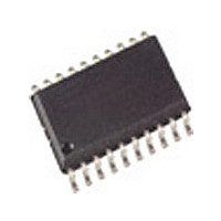
T5743N-TG Atmel, T5743N-TG Datasheet - Page 6

T5743N-TG
Manufacturer Part Number
T5743N-TG
Description
Manufacturer
Atmel
Datasheet
1.T5743N-TG.pdf
(34 pages)
Specifications of T5743N-TG
Operating Frequency (max)
450000kHz
Operating Temperature (min)
-40C
Operating Temperature (max)
105C
Operating Temperature Classification
Industrial
Operating Supply Voltage (min)
4.5V
Operating Supply Voltage (typ)
5V
Operating Supply Voltage (max)
5.5V
Lead Free Status / Rohs Status
Not Compliant
RSSI Amplifier
The subsequent RSSI amplifier enhances the output
signal of the IF amplifier before it is fed into the demod-
ulator. The dynamic range of this amplifier is
DR
its linear range, the best S/N ratio is maintained in ASK
mode. If the dynamic range is exceeded by the transmitter
signal, the S/N ratio is defined by the ratio of the maxi-
mum RSSI output voltage and the RSSI output voltage
due to a disturber. The dynamic range of the RSSI ampli-
fier is exceeded if the RF input signal is about 60 dB
higher compared to the RF input signal at full sensitivity.
In FSK mode the S/N ratio is not affected by the dynamic
range of the RSSI amplifier.
The output voltage of the RSSI amplifier is internally
compared to a threshold voltage V
mined by the value of the external resistor R
connected between Pin SENS and GND or V
of the comparator is fed into the digital control logic. By
this means it is possible to operate the receiver at a lower
sensitivity.
If R
sensitivity.
If R
lower sensitivity. The reduced sensitivity is defined by the
value of R
noise ratio of the LNA input. The reduced sensitivity
depends on the signal strength at the output of the RSSI
amplifier.
Since different RF input networks may exhibit slightly
different values for the LNA gain, the sensitivity values
given in the electrical characteristics refer to a specific
input matching. This matching is illustrated in figure 6
and exhibits the best possible sensitivity.
R
receiver can be switched from full sensitivity to reduced
sensitivity or vice versa at any time. In polling mode, the
receiver will not wake up if the RF input signal does not
exceed the selected sensitivity. If the receiver is already
active, the data stream at Pin DATA will disappear when
the input signal is lower than defined by the reduced
sensitivity. Instead of the data stream, the pattern accord-
ing to figure 7 is issued at Pin DATA to indicate that the
receiver is still active (see also figure 34).
T5743N
6 (34)
Sens
DATA
RSSI
Sens
Sens
Figure 7. Steady L state limited DATA output pattern
can be connected to V
is connected to GND, the receiver operates at full
= 60 dB. If the RSSI amplifier is operated within
is connected to V
Sens
t
DATA_min
, the maximum sensitivity by the signal-to-
t DATA_L_max
S
, the receiver operates at a
S
or GND via a C. The
Th_red
. V
Th_red
S
Sens
. The output
. R
is deter-
Sens
is
FSK/ASK Demodulator and Data Filter
The signal coming from the RSSI amplifier is converted
into the raw data signal by the ASK/FSK demodulator.
The operating mode of the demodulator is set via the bit
ASK/_FSK in the OPMODE register. Logic ‘L’ sets the
demodulator to FSK, applying ‘H’ to ASK mode.
In ASK mode, an automatic threshold control circuit
(ATC) is used to set the detection reference voltage to a
value where a good signal-to-noise ratio is achieved. This
circuit effectively suppresses any kind of inband noise
signals or competing transmitters. If the S/N (ratio to sup-
press inband noise signals) exceeds 10 dB, the data signal
can be detected properly.
The FSK demodulator is intended to be used for an FSK
deviation of 10 kHz
data signal can be detected if the S/N (ratio to suppress
inband noise signals) exceeds 2 dB. This value is guaran-
teed for all modulation schemes of a disturber signal.
The output signal of the demodulator is filtered by the
data filter before it is fed into the digital signal processing
circuit. The data filter improves the S/N ratio as its pass-
band can be adopted to the characteristics of the data
signal. The data filter consists of a 1
a 2
The highpass filter cut-off frequency is defined by an
external capacitor connected to Pin CDEM. The cut-off
frequency of the highpass filter is defined by the follow-
ing formula:
fcu_DF +
In self-polling mode, the data filter must settle very
rapidly to achieve a low current consumption. Therefore,
CDEM cannot be increased to very high values if self-
polling is used. On the other hand CDEM must be large
enough to meet the data filter requirements according to
the data signal. Recommended values for CDEM are
given in the electrical characteristics.
The cut-off frequency of the lowpass filter is defined by
the
BR_Range is defined in the OPMODE register (refer to
chapter ‘Configuration of the Receiver’). The BR_Range
must be set in accordance to the used baud rate.
nd
-order lowpass filter
selected
2
p
baud-rate
30 kW
Df
1
range
100 kHz. In FSK mode the
CDEM
st
Rev. A3, 17-Dec-01
(BR_Range).
-order highpass and
The


