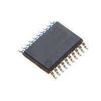
ATTINY861A-XU Atmel, ATTINY861A-XU Datasheet - Page 125

ATTINY861A-XU
Manufacturer Part Number
ATTINY861A-XU
Description
Microcontrollers (MCU) 8K Flash;125B EEPROM 128B SRAM;16 IO Pins
Manufacturer
Atmel
Datasheet
1.ATTINY861A-XU.pdf
(292 pages)
Specifications of ATTINY861A-XU
Core
RISC
Data Bus Width
8 bit
Program Memory Type
Flash
Program Memory Size
8 KB
Data Ram Size
512 B
Interface Type
SPI
Maximum Clock Frequency
20 MHz
Number Of Programmable I/os
16
Operating Supply Voltage
1.8 V to 5.5 V
Maximum Operating Temperature
+ 85 C
Mounting Style
SMD/SMT
Package / Case
TSSOP-20
Minimum Operating Temperature
- 40 C
Lead Free Status / Rohs Status
Details
Available stocks
Company
Part Number
Manufacturer
Quantity
Price
Company:
Part Number:
ATTINY861A-XUR
Manufacturer:
IDT
Quantity:
1 300
- Current page: 125 of 292
- Download datasheet (9Mb)
13.3.2
8197B–AVR–01/10
SPI Master Operation Example
Figure 13-3. Three-wire Mode, Timing Diagram
The Three-wire mode timing is shown in Figure 13-3. At the top of the figure is a USCK cycle ref-
erence. One bit is shifted into the USI Data Register (USIDR) for each of these cycles. The
USCK timing is shown for both external clock modes. In External Clock mode 0 (USICS0 = 0), DI
is sampled at positive edges, and DO is changed (Data Register is shifted by one) at negative
edges. In external clock mode 1 (USICS0 = 1) the opposite edges with respect to mode 0 are
used. In other words, data is sampled at negative and output is changed at positive edges. The
USI clock modes corresponds to the SPI data mode 0 and 1.
Referring to the timing diagram
The following code demonstrates how to use the USI module as a SPI Master:
CYCLE
1. The slave and master devices set up their data outputs and, depending on the protocol
2. The master software generates a clock pulse by toggling the USCK line twice (C and
3. Step 2. is repeated eight times for a complete register (byte) transfer.
4. After eight clock pulses (i.e., 16 clock edges) the counter will overflow and indicate that
USCK
USCK
SPITransfer:
SPITransfer_loop:
DO
DI
used, enable their output drivers (mark A and B). The output is set up by writing the
data to be transmitted to the USI Data Register. The output is enabled by setting the
corresponding bit in the Data Direction Register of Port A. Note that there is not a pre-
ferred order of points A and B in the figure, but both must be at least one half USCK
cycle before point C, where the data is sampled. This is in order to ensure that the data
setup requirement is satisfied. The 4-bit counter is reset to zero.
D). The bit values on the data input (DI) pins are sampled by the USI on the first edge
(C), and the data output is changed on the opposite edge (D). The 4-bit counter will
count both edges.
the transfer has been completed. The data bytes transferred must now be processed
before a new transfer can be initiated. The overflow interrupt will wake up the processor
if it is set to Idle mode. Depending on the protocol used the slave device can now set its
output to high impedance.
sts
ldi
sts
ldi
sts
lds
( Reference )
A
USIDR,r16
r16,(1<<USIOIF)
USISR,r16
r16,(1<<USIWM0)|(1<<USICS1)|(1<<USICLK)|(1<<USITC)
USICR,r16
r16, USISR
B
MSB
MSB
C
1
D
2
6
6
(Figure
3
5
5
13-3), a bus transfer involves the following steps:
4
4
4
5
3
3
6
2
2
7
1
1
LSB
LSB
8
E
125
Related parts for ATTINY861A-XU
Image
Part Number
Description
Manufacturer
Datasheet
Request
R

Part Number:
Description:
DEV KIT FOR AVR/AVR32
Manufacturer:
Atmel
Datasheet:

Part Number:
Description:
INTERVAL AND WIPE/WASH WIPER CONTROL IC WITH DELAY
Manufacturer:
ATMEL Corporation
Datasheet:

Part Number:
Description:
Low-Voltage Voice-Switched IC for Hands-Free Operation
Manufacturer:
ATMEL Corporation
Datasheet:

Part Number:
Description:
MONOLITHIC INTEGRATED FEATUREPHONE CIRCUIT
Manufacturer:
ATMEL Corporation
Datasheet:

Part Number:
Description:
AM-FM Receiver IC U4255BM-M
Manufacturer:
ATMEL Corporation
Datasheet:

Part Number:
Description:
Monolithic Integrated Feature Phone Circuit
Manufacturer:
ATMEL Corporation
Datasheet:

Part Number:
Description:
Multistandard Video-IF and Quasi Parallel Sound Processing
Manufacturer:
ATMEL Corporation
Datasheet:

Part Number:
Description:
High-performance EE PLD
Manufacturer:
ATMEL Corporation
Datasheet:

Part Number:
Description:
8-bit Flash Microcontroller
Manufacturer:
ATMEL Corporation
Datasheet:

Part Number:
Description:
2-Wire Serial EEPROM
Manufacturer:
ATMEL Corporation
Datasheet:


