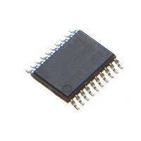
ATTINY861A-XU Atmel, ATTINY861A-XU Datasheet - Page 98

ATTINY861A-XU
Manufacturer Part Number
ATTINY861A-XU
Description
Microcontrollers (MCU) 8K Flash;125B EEPROM 128B SRAM;16 IO Pins
Manufacturer
Atmel
Datasheet
1.ATTINY861A-XU.pdf
(292 pages)
Specifications of ATTINY861A-XU
Core
RISC
Data Bus Width
8 bit
Program Memory Type
Flash
Program Memory Size
8 KB
Data Ram Size
512 B
Interface Type
SPI
Maximum Clock Frequency
20 MHz
Number Of Programmable I/os
16
Operating Supply Voltage
1.8 V to 5.5 V
Maximum Operating Temperature
+ 85 C
Mounting Style
SMD/SMT
Package / Case
TSSOP-20
Minimum Operating Temperature
- 40 C
Lead Free Status / Rohs Status
Details
Available stocks
Company
Part Number
Manufacturer
Quantity
Price
Company:
Part Number:
ATTINY861A-XUR
Manufacturer:
IDT
Quantity:
1 300
- Current page: 98 of 292
- Download datasheet (9Mb)
12.8.2
98
ATtiny261A/461A/861A
Fast PWM Mode
The counter value (TCNT1) that is shown as a histogram in
counter value matches the TOP value. The counter is then cleared at the following clock cycle
The diagram includes the Waveform Output (OCW1x) in toggle Compare Mode. The small hori-
zontal line marks on the TCNT1 slopes represent Compare Matches between OCR1x and
TCNT1.
The Timer/Counter Overflow Flag (TOV1) is set in the same clock cycle as the TCNT1 becomes
zero. The TOV1 Flag in this case behaves like a 11th bit, except that it is only set, not cleared.
However, combined with the timer overflow interrupt, that automatically clears the TOV1 Flag,
the timer resolution can be increased by software. There are no special cases to consider in the
Normal mode, a new counter value can be written anytime.
The Output Compare Unit can be used to generate interrupts at some given time. Using the Out-
put Compare to generate waveforms in Normal mode is not recommended, since this will
occupy too much of the CPU time. For generating a waveform, the OCW1x output can be set to
toggle its logical level on each Compare Match by setting the Compare Output mode bits to tog-
gle mode (COM1x1:0 = 1). The OC1x value will not be visible on the port pin unless the data
direction for the pin is set to output. The waveform generated will have a maximum frequency of
f
equation:
Resolution, R
and it can be calculated using the following equation:
The Output Compare Pin configurations in Normal Mode are described in
Table 12-2.
The fast Pulse Width Modulation or fast PWM mode (PWM1A/PWM1B = 1 and WGM11:10 = 00)
provides a high frequency PWM waveform generation option. The fast PWM differs from the
other PWM option by its single-slope operation. The counter counts from BOTTOM to TOP
(defined as OCR1C) then restarts from BOTTOM. In non-inverting Compare Output mode the
Waveform Output (OCW1x) is cleared on the Compare Match between TCNT1 and OCR1x and
set at BOTTOM. In inverting Compare Output mode, the Waveform Output is set on Compare
Match and cleared at BOTTOM. In complementary Compare Output mode the Waveform Output
is cleared on the Compare Match and set at BOTTOM.
Due to the single-slope operation, the operating frequency of the fast PWM mode can be twice
as high as the Phase and Frequency Correct PWM mode that use dual-slope operation. This
high frequency makes the fast PWM mode well suited for power regulation, rectification, and
OC1x
COM1x1
0
0
1
1
= f
clkT1
/4 when OCR1C is set to zero. The waveform frequency is defined by the following
PWM
Output Compare Pin Configurations in Normal Mode
, shows how many bit is required to express the value in the OCR1C register
COM1x0
0
1
0
1
f
OC1x
R
PWM
OC1x Pin
Disconnected
Disconnected
Disconnected
Disconnected
=
=
------------------------------------------ -
2
⋅
log
(
1
2
f
+
clkT1
(
OCR1C
OCR1C
)
+
1
Figure 12-11
)
OC1x Pin
Disconnected
OC1x
OC1x
OC1x
is incremented until the
Table
12-2.
8197B–AVR–01/10
Related parts for ATTINY861A-XU
Image
Part Number
Description
Manufacturer
Datasheet
Request
R

Part Number:
Description:
DEV KIT FOR AVR/AVR32
Manufacturer:
Atmel
Datasheet:

Part Number:
Description:
INTERVAL AND WIPE/WASH WIPER CONTROL IC WITH DELAY
Manufacturer:
ATMEL Corporation
Datasheet:

Part Number:
Description:
Low-Voltage Voice-Switched IC for Hands-Free Operation
Manufacturer:
ATMEL Corporation
Datasheet:

Part Number:
Description:
MONOLITHIC INTEGRATED FEATUREPHONE CIRCUIT
Manufacturer:
ATMEL Corporation
Datasheet:

Part Number:
Description:
AM-FM Receiver IC U4255BM-M
Manufacturer:
ATMEL Corporation
Datasheet:

Part Number:
Description:
Monolithic Integrated Feature Phone Circuit
Manufacturer:
ATMEL Corporation
Datasheet:

Part Number:
Description:
Multistandard Video-IF and Quasi Parallel Sound Processing
Manufacturer:
ATMEL Corporation
Datasheet:

Part Number:
Description:
High-performance EE PLD
Manufacturer:
ATMEL Corporation
Datasheet:

Part Number:
Description:
8-bit Flash Microcontroller
Manufacturer:
ATMEL Corporation
Datasheet:

Part Number:
Description:
2-Wire Serial EEPROM
Manufacturer:
ATMEL Corporation
Datasheet:


