ATTINY861A-XU Atmel, ATTINY861A-XU Datasheet - Page 143
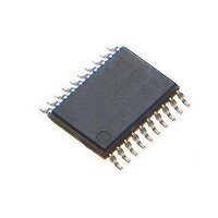
ATTINY861A-XU
Manufacturer Part Number
ATTINY861A-XU
Description
Microcontrollers (MCU) 8K Flash;125B EEPROM 128B SRAM;16 IO Pins
Manufacturer
Atmel
Datasheet
1.ATTINY861A-XU.pdf
(292 pages)
Specifications of ATTINY861A-XU
Core
RISC
Data Bus Width
8 bit
Program Memory Type
Flash
Program Memory Size
8 KB
Data Ram Size
512 B
Interface Type
SPI
Maximum Clock Frequency
20 MHz
Number Of Programmable I/os
16
Operating Supply Voltage
1.8 V to 5.5 V
Maximum Operating Temperature
+ 85 C
Mounting Style
SMD/SMT
Package / Case
TSSOP-20
Minimum Operating Temperature
- 40 C
Lead Free Status / Rohs Status
Details
Available stocks
Company
Part Number
Manufacturer
Quantity
Price
Company:

Part Number:
ATTINY861A-XUR
Manufacturer:
IDT
Quantity:
1 300


15.5
8197B–AVR–01/10
Prescaling and Conversion Timing
conversion will not be started. If another positive edge occurs on the trigger signal during con-
version, the edge will be ignored. Note that an Interrupt Flag will be set even if the specific
interrupt is disabled or the Global Interrupt Enable bit in SREG is cleared. A conversion can thus
be triggered without causing an interrupt. However, the Interrupt Flag must be cleared in order to
trigger a new conversion at the next interrupt event.
Figure 15-2. ADC Auto Trigger Logic
Using the ADC Interrupt Flag as a trigger source makes the ADC start a new conversion as soon
as the ongoing conversion has finished. The ADC then operates in Free Running mode, con-
stantly sampling and updating the ADC Data Register. The first conversion must be started by
writing a logical one to the ADSC bit in ADCSRA. In this mode the ADC will perform successive
conversions independently of whether the ADC Interrupt Flag, ADIF is cleared or not.
If Auto Triggering is enabled, single conversions can be started by writing ADSC in ADCSRA to
one. ADSC can also be used to determine if a conversion is in progress. The ADSC bit will be
read as one during a conversion, independently of how the conversion was started.
By default, the successive approximation circuitry requires an input clock frequency between 50
kHz and 200 kHz to get maximum resolution. If a lower resolution than 10 bits is needed, the
input clock frequency to the ADC can be higher than 200 kHz to get a higher sample rate.
Figure 15-3. ADC Prescaler
ADSC
SOURCE n
ADIF
SOURCE 1
.
.
.
.
ADTS[2:0]
ADEN
START
ADPS0
ADPS1
ADPS2
DETECTOR
CK
EDGE
Reset
ADATE
7-BIT ADC PRESCALER
ADC CLOCK SOURCE
START
CONVERSION
PRESCALER
LOGIC
CLK
ADC
143
Related parts for ATTINY861A-XU
Image
Part Number
Description
Manufacturer
Datasheet
Request
R

Part Number:
Description:
DEV KIT FOR AVR/AVR32
Manufacturer:
Atmel
Datasheet:

Part Number:
Description:
INTERVAL AND WIPE/WASH WIPER CONTROL IC WITH DELAY
Manufacturer:
ATMEL Corporation
Datasheet:
Part Number:
Description:
Low-Voltage Voice-Switched IC for Hands-Free Operation
Manufacturer:
ATMEL Corporation
Datasheet:
Part Number:
Description:
MONOLITHIC INTEGRATED FEATUREPHONE CIRCUIT
Manufacturer:
ATMEL Corporation
Datasheet:
Part Number:
Description:
AM-FM Receiver IC U4255BM-M
Manufacturer:
ATMEL Corporation
Datasheet:
Part Number:
Description:
Monolithic Integrated Feature Phone Circuit
Manufacturer:
ATMEL Corporation
Datasheet:
Part Number:
Description:
Multistandard Video-IF and Quasi Parallel Sound Processing
Manufacturer:
ATMEL Corporation
Datasheet:
Part Number:
Description:
High-performance EE PLD
Manufacturer:
ATMEL Corporation
Datasheet:
Part Number:
Description:
8-bit Flash Microcontroller
Manufacturer:
ATMEL Corporation
Datasheet:
Part Number:
Description:
2-Wire Serial EEPROM
Manufacturer:
ATMEL Corporation
Datasheet: