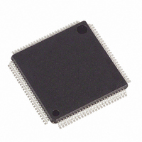
DS21552L+ Maxim Integrated Products, DS21552L+ Datasheet - Page 102

DS21552L+
Manufacturer Part Number
DS21552L+
Description
IC TXRX T1 1-CHIP 5V 100-LQFP
Manufacturer
Maxim Integrated Products
Datasheet
1.DS21352L.pdf
(137 pages)
Specifications of DS21552L+
Function
Single-Chip Transceiver
Interface
E1, HDLC, J1, T1
Number Of Circuits
1
Voltage - Supply
4.75 V ~ 5.25 V
Current - Supply
75mA
Operating Temperature
0°C ~ 70°C
Mounting Type
Surface Mount
Package / Case
100-LQFP
Includes
DSX-1 and CSU Line Build-Out Generator, HDLC Controller, In-Band Loop Code Generator and Detector
Product
Framer
Number Of Transceivers
1
Data Rate
64 Kbps
Supply Voltage (max)
3.465 V
Supply Voltage (min)
3.135 V
Supply Current (max)
75 mA (Typ)
Maximum Operating Temperature
+ 70 C
Minimum Operating Temperature
0 C
Mounting Style
SMD/SMT
Ic Interface Type
Parallel, Serial
Supply Voltage Range
4.75V To 5.25V
Operating Temperature Range
0°C To +70°C
Digital Ic Case Style
LQFP
No. Of Pins
100
Filter Terminals
SMD
Rohs Compliant
Yes
Lead Free Status / RoHS Status
Lead free / RoHS Compliant
Power (watts)
-
Lead Free Status / Rohs Status
Lead free / RoHS Compliant
Table 19-1 INSTRUCTION CODES FOR IEEE 1149.1 ARCHITECTURE
Instruction
SAMPLE/PRELOAD
BYPASS
EXTEST
CLAMP
HIGHZ
IDCODE
SAMPLE/PRELOAD
This is a mandatory instruction for the IEEE 1149.1 specification.
functions. The digital I/Os of the device can be sampled at the boundary scan register without interfering
with the normal operation of the device by using the Capture-DR state. SAMPLE/PRELOAD also allows
the device to shift data into the boundary scan register via JTDI using the Shift-DR state.
BYPASS
When the BYPASS instruction is latched into the parallel instruction register, JTDI connects to JTDO
through the one-bit bypass test register. This allows data to pass from JTDI to JTDO not affecting the
device’s normal operation.
EXTEST
This allows testing of all interconnections to the device. When the EXTEST instruction is latched in the
instruction register, the following actions occur. Once enabled via the Update-IR state, the parallel
outputs of all digital output pins will be driven. The boundary scan register will be connected between
JTDI and JTDO. The Capture-DR will sample all digital inputs into the boundary scan register.
CLAMP
All digital outputs of the device will output data from the boundary scan parallel output while connecting
the bypass register between JTDI and JTDO. The outputs will not change during the CLAMP instruction.
HIGHZ
All digital outputs of the device will be placed in a high impedance state. The BYPASS register will be
connected between JTDI and JTDO.
EXIT2-IR
A rising edge on JTCLK with JTMS LOW will put the controller in the Update-IR state. The controller
will loop back to Shift-IR if JTMS is HIGH during a rising edge of JTCLK in this state.
UPDATE-IR
The instruction code shifted into the instruction shift register is latched into the parallel output on the
falling edge of JTCLK as the controller enters this state. Once latched, this instruction becomes the
current instruction. A rising edge on JTCLK with JTMS LOW, will put the controller in the Run-Test-
Idle state. With JTMS HIGH, the controller will enter the Select-DR-Scan state.
Selected Register
Boundary Scan
Bypass
Boundary Scan
Bypass
Bypass
Device Identification
102 of 137
Instruction Codes
010
111
000
011
100
001
This instruction supports two
DS21352/DS21552


