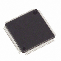
DS21552L+ Maxim Integrated Products, DS21552L+ Datasheet - Page 35

DS21552L+
Manufacturer Part Number
DS21552L+
Description
IC TXRX T1 1-CHIP 5V 100-LQFP
Manufacturer
Maxim Integrated Products
Datasheet
1.DS21352L.pdf
(137 pages)
Specifications of DS21552L+
Function
Single-Chip Transceiver
Interface
E1, HDLC, J1, T1
Number Of Circuits
1
Voltage - Supply
4.75 V ~ 5.25 V
Current - Supply
75mA
Operating Temperature
0°C ~ 70°C
Mounting Type
Surface Mount
Package / Case
100-LQFP
Includes
DSX-1 and CSU Line Build-Out Generator, HDLC Controller, In-Band Loop Code Generator and Detector
Product
Framer
Number Of Transceivers
1
Data Rate
64 Kbps
Supply Voltage (max)
3.465 V
Supply Voltage (min)
3.135 V
Supply Current (max)
75 mA (Typ)
Maximum Operating Temperature
+ 70 C
Minimum Operating Temperature
0 C
Mounting Style
SMD/SMT
Ic Interface Type
Parallel, Serial
Supply Voltage Range
4.75V To 5.25V
Operating Temperature Range
0°C To +70°C
Digital Ic Case Style
LQFP
No. Of Pins
100
Filter Terminals
SMD
Rohs Compliant
Yes
Lead Free Status / RoHS Status
Lead free / RoHS Compliant
Power (watts)
-
Lead Free Status / Rohs Status
Lead free / RoHS Compliant
CCR1: COMMON CONTROL REGISTER 1 (Address=37 Hex)
6.3 PAYLOAD LOOPBACK
Payload Loopback When CCR1.1 is set to a one, the DS21352/552 will be forced into Payload LoopBack
(PLB). Normally, this loopback is only enabled when ESF framing is being performed but can be enabled
also in D4 framing applications. In a PLB situation, the DS21352/552 will loop the 192 bits of pay-load
data (with BPVs corrected) from the receive section back to the transmit section. The FPS framing pat-
tern, CRC6 calculation, and the FDL bits are not looped back, they are reinserted by the DS21352/552.
When PLB is enabled, the following will occur:
1. data will be transmitted from the TPOSO and TNEGO pins synchronous with RCLK instead of TCLK
2. all of the receive side signals will continue to operate normally
3. the TCHCLK and TCHBLK signals are forced low
4. data at the TSER, TDATA, and TSIG pins is ignored
5. the TLCLK signal will become synchronous with RCLK instead of TCLK.
6.4 FRAMER LOOPBACK
When CCR1.0 is set to a one, the DS21352/552 will enter a Framer LoopBack (FLB) mode. This
loopback is useful in testing and debugging applications. In FLB, the DS21352/552 will loop data from
the transmit side back to the receive side. When FLB is enabled, the following will occur:
1. An unframed all one’s code will be transmitted at TPOSO and TNEGO
2. Data at RPOSI and RNEGI will be ignored
SYMBOL
RSCLKM
TSCLKM
(MSB)
TESE
RSAO
TESE
RESE
ODF
PLB
FLB
POSITION
ODF
CCR1.7
CCR1.6
CCR1.5
CCR1.4
CCR1.3
CCR1.2
CCR1.1
CCR1.0
RSAO
NAME AND DESCRIPTION
Transmit Elastic Store Enable.
0 = elastic store is bypassed
1 = elastic store is enabled
Output Data Format.
0 = bipolar data at TPOSO and TNEGO
1 = NRZ data at TPOSO; TNEGO = 0
Receive Signaling All One’s. This bit should not be enabled if hardware signaling is
being utilized. See Section 10 for more details.
0 = allow robbed signaling bits to appear at RSER
1 = force all robbed signaling bits at RSER to one
TSYSCLK Mode Select.
0 = if TSYSCLK is 1.544 MHz
1 = if TSYSCLK is 2.048 MHz or IBO enabled (see section 20 for details on IBO
function)
RSYSCLK Mode Select.
0 = if RSYSCLK is 1.544 MHz
1 = if RSYSCLK is 2.048 MHz or IBO enabled (see section 20 for details on IBO
function)
Receive Elastic Store Enable.
0 = elastic store is bypassed
1 = elastic store is enabled
Payload Loopback.
0 = loopback disabled
1 = loopback enabled
Framer Loopback.
0 = loopback disabled
1 = loopback enabled
TSCLKM
35 of 137
RSCLKM
RESE
PLB
(LSB)
FLB


