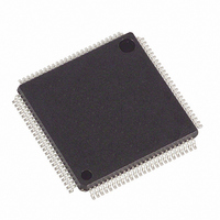
DS21552L+ Maxim Integrated Products, DS21552L+ Datasheet - Page 81

DS21552L+
Manufacturer Part Number
DS21552L+
Description
IC TXRX T1 1-CHIP 5V 100-LQFP
Manufacturer
Maxim Integrated Products
Datasheet
1.DS21352L.pdf
(137 pages)
Specifications of DS21552L+
Function
Single-Chip Transceiver
Interface
E1, HDLC, J1, T1
Number Of Circuits
1
Voltage - Supply
4.75 V ~ 5.25 V
Current - Supply
75mA
Operating Temperature
0°C ~ 70°C
Mounting Type
Surface Mount
Package / Case
100-LQFP
Includes
DSX-1 and CSU Line Build-Out Generator, HDLC Controller, In-Band Loop Code Generator and Detector
Product
Framer
Number Of Transceivers
1
Data Rate
64 Kbps
Supply Voltage (max)
3.465 V
Supply Voltage (min)
3.135 V
Supply Current (max)
75 mA (Typ)
Maximum Operating Temperature
+ 70 C
Minimum Operating Temperature
0 C
Mounting Style
SMD/SMT
Ic Interface Type
Parallel, Serial
Supply Voltage Range
4.75V To 5.25V
Operating Temperature Range
0°C To +70°C
Digital Ic Case Style
LQFP
No. Of Pins
100
Filter Terminals
SMD
Rohs Compliant
Yes
Lead Free Status / RoHS Status
Lead free / RoHS Compliant
Power (watts)
-
Lead Free Status / Rohs Status
Lead free / RoHS Compliant
The framer also contains a zero destuffer which is controlled via the CCR2.0 bit. In both ANSI T1.403
and TR54016, communications on the FDL follows a subset of a LAPD protocol. The LAPD protocol
states that no more than 5 ones should be transmitted in a row so that the data does not resemble an
opening or closing flag (01111110) or an abort signal (11111111). If enabled via CCR2.0, the
DS21352/552 will automatically look for 5 ones in a row, followed by a zero. If it finds such a pattern, it
will automatically remove the zero. If the zero destuffer sees six or more ones in a row followed by a
zero, the zero is not removed. The CCR2.0 bit should always be set to a one when the DS21352/552 is
extracting the FDL. More on how to use the DS21352/552 in FDL applications in this legacy support
mode is covered in a separate Application Note.
RFDL: RECEIVE FDL REGISTER (Address=28 Hex)
The Receive FDL Register (RFDL) reports the incoming Facility Data Link (FDL) or the incoming Fs bits. The LSB is
received first.
RFDLM1: RECEIVE FDL MATCH REGISTER 1 (Address=29 Hex)
RFDLM2: RECEIVE FDL MATCH REGISTER 2 (Address=2A Hex)
When the byte in the Receive FDL Register matches either of the two Receive FDL Match Registers (RFDLM1/RFDLM2),
SR2.2 will be set to a one and the INT will go active if enabled via IMR2.2.
SYMBOL
SYMBOL
RFDL7
RFDL7
(MSB)
(MSB)
RFDL7
RFDL0
RFDL7
RFDL0
RFDL6
RFDL6
POSITION
POSITION
RFDL.7
RFDL.0
RFDL.7
RFDL.0
RFDL5
RFDL5
NAME AND DESCRIPTION
NAME AND DESCRIPTION
MSB of the Received FDL Code
LSB of the Received FDL Code
MSB of the FDL Match Code
LSB of the FDL Match Code
RFDL4
RFDL4
81 of 137
RFDL3
RFDL3
RFDL2
RFDL2
RFDL1
RFDL1
RFDL0
RFDL0
(LSB)
(LSB)


