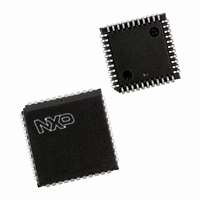
SC16C2552BIA44,529 NXP Semiconductors, SC16C2552BIA44,529 Datasheet - Page 18

SC16C2552BIA44,529
Manufacturer Part Number
SC16C2552BIA44,529
Description
IC UART DUAL W/FIFO 44-PLCC
Manufacturer
NXP Semiconductors
Type
Dual UART with 16-byte FIFOsr
Datasheet
1.SC16C2552BIA44529.pdf
(38 pages)
Specifications of SC16C2552BIA44,529
Number Of Channels
2, DUART
Package / Case
44-LCC (J-Lead)
Features
2 Channels
Fifo's
16 Byte
Voltage - Supply
2.5V, 3.3V, 5V
With Irda Encoder/decoder
Yes
With False Start Bit Detection
Yes
With Modem Control
Yes
With Cmos
Yes
Mounting Type
Surface Mount
Data Rate
5 Mbps
Supply Voltage (max)
5.5 V
Supply Voltage (min)
2.25 V
Supply Current
4.5 mA
Maximum Operating Temperature
+ 85 C
Minimum Operating Temperature
- 40 C
Mounting Style
SMD/SMT
Operating Supply Voltage
2.5 V or 3.3 V or 5 V
Lead Free Status / RoHS Status
Lead free / RoHS Compliant
Lead Free Status / RoHS Status
Lead free / RoHS Compliant, Lead free / RoHS Compliant
Other names
568-3646-5
935274408529
SC16C2552BIA44-S
935274408529
SC16C2552BIA44-S
Available stocks
Company
Part Number
Manufacturer
Quantity
Price
Company:
Part Number:
SC16C2552BIA44,529
Manufacturer:
NXP Semiconductors
Quantity:
10 000
NXP Semiconductors
SC16C2552B_3
Product data sheet
7.6 Modem Control Register (MCR)
This register controls the interface with the modem or a peripheral device.
Table 16.
Bit
7:5
4
3
2
1
0
Symbol
MCR[7:5]
MCR[4]
MCR[3]
MCR[2]
MCR[1]
MCR[0]
Modem Control Register bits description
5 V, 3.3 V and 2.5 V dual UART, 5 Mbit/s (max.), with 16-byte FIFOs
Description
reserved; initialized to a logic 0
Loopback. Enable the local Loopback mode (diagnostics). In this mode the
transmitter output (TX) and the receiver input (RX), CTS, DSR, CD and RI
are disconnected from the SC16C2552B I/O pins. Internally the modem
data and control pins are connected into a loopback data configuration
(see
fully operational. The modem control interrupts are also operational, but
the interrupts’ sources are switched to the lower four bits of the Modem
Control. Interrupts continue to be controlled by the IER register.
OP2. Used to control the modem CD signal in the Loopback mode.
OP1. This bit is used in the Loopback mode only. In the Loopback mode,
this bit is used to write the state of the modem RI interface signal.
RTS
DTR
Rev. 03 — 12 February 2009
logic 0 = disable Loopback mode (normal default condition)
logic 1 = enable local Loopback mode (diagnostics)
logic 0 = sets OP2 to a logic 1 (normal default condition). In the
Loopback mode, sets CD internally to a logic 1.
logic 1 = sets OP2 to a logic 0. In the Loopback mode, sets CD internally
to a logic 0.
logic 0 = force RTS output to a logic 1 (normal default condition)
logic 1 = force RTS output to a logic 0
logic 0 = force DTR output to a logic 1 (normal default condition)
logic 1 = force DTR output to a logic 0
Figure
4). In this mode, the receiver and transmitter interrupts remain
SC16C2552B
© NXP B.V. 2009. All rights reserved.
18 of 38


