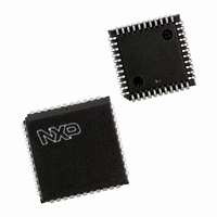
SC16C2552BIA44,529 NXP Semiconductors, SC16C2552BIA44,529 Datasheet - Page 3

SC16C2552BIA44,529
Manufacturer Part Number
SC16C2552BIA44,529
Description
IC UART DUAL W/FIFO 44-PLCC
Manufacturer
NXP Semiconductors
Type
Dual UART with 16-byte FIFOsr
Datasheet
1.SC16C2552BIA44529.pdf
(38 pages)
Specifications of SC16C2552BIA44,529
Number Of Channels
2, DUART
Package / Case
44-LCC (J-Lead)
Features
2 Channels
Fifo's
16 Byte
Voltage - Supply
2.5V, 3.3V, 5V
With Irda Encoder/decoder
Yes
With False Start Bit Detection
Yes
With Modem Control
Yes
With Cmos
Yes
Mounting Type
Surface Mount
Data Rate
5 Mbps
Supply Voltage (max)
5.5 V
Supply Voltage (min)
2.25 V
Supply Current
4.5 mA
Maximum Operating Temperature
+ 85 C
Minimum Operating Temperature
- 40 C
Mounting Style
SMD/SMT
Operating Supply Voltage
2.5 V or 3.3 V or 5 V
Lead Free Status / RoHS Status
Lead free / RoHS Compliant
Lead Free Status / RoHS Status
Lead free / RoHS Compliant, Lead free / RoHS Compliant
Other names
568-3646-5
935274408529
SC16C2552BIA44-S
935274408529
SC16C2552BIA44-S
Available stocks
Company
Part Number
Manufacturer
Quantity
Price
Company:
Part Number:
SC16C2552BIA44,529
Manufacturer:
NXP Semiconductors
Quantity:
10 000
NXP Semiconductors
5. Pinning information
Table 2.
SC16C2552B_3
Product data sheet
Symbol
A0
A1
A2
CDA
CDB
CHSEL
CTSA
CTSB
CS
Pin description
Pin
10
14
15
42
30
16
40
28
18
5.1 Pinning
5.2 Pin description
Type
I
I
I
I
I
I
I
I
I
Fig 2.
Description
Register select. A0 to A2 are used during read and write operations to select the UART
register to read from or write to.
Carrier detect A, B (active LOW). These inputs are associated with individual UART
channels A through B. A logic 0 on this pin indicates that a carrier has been detected by the
modem for that channel.
Channel select. UART channel A or B is selected by the logic state of this pin when CS is a
logic 0. A logic 0 on CHSEL selects the UART channel B, while a logic 1 selects UART
channel A. Bit 0 of AFR register can temporarily override CHSEL function, allowing user to
write to both channel registers simultaneously with one write cycle.
Clear to Send A, B (active LOW). These inputs are associated with individual UART
channels A through B. A logic 0 on the CTSn pin indicates the modem or data set is ready to
accept transmit data from the SC16C2552B. Status can be tested by reading MSR[4].
Chip select (active LOW). This function selects channel A or channel B in accordance with
the logical state of the CHSEL pin. This allows data to be transferred between the user CPU
and the SC16C2552B.
Pin configuration for PLCC44
CHSEL
XTAL1
XTAL2
5 V, 3.3 V and 2.5 V dual UART, 5 Mbit/s (max.), with 16-byte FIFOs
INTB
GND
D5
D6
D7
A0
A1
A2
Rev. 03 — 12 February 2009
10
11
12
13
14
15
16
17
7
8
9
SC16C2552BIA44
002aaa488
SC16C2552B
39
38
37
36
35
34
33
32
31
30
29
RXA
TXA
DTRA
RTSA
MFA
INTA
V
TXRDYB
RIB
CDB
DSRB
CC
© NXP B.V. 2009. All rights reserved.
3 of 38


