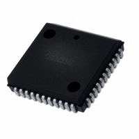
IS82C50A-5 Intersil, IS82C50A-5 Datasheet - Page 5

IS82C50A-5
Manufacturer Part Number
IS82C50A-5
Description
IC PERIPH UART/BRG 10MHZ 44-PLCC
Manufacturer
Intersil
Datasheet
1.CS82C50A-5Z.pdf
(25 pages)
Specifications of IS82C50A-5
Features
Single Chip UART/BRG
Number Of Channels
1, UART
Protocol
RS232C
Voltage - Supply
4.5 V ~ 5.5 V
With Parallel Port
Yes
With False Start Bit Detection
Yes
With Modem Control
Yes
With Cmos
Yes
Mounting Type
Surface Mount
Package / Case
44-LCC (J-Lead)
Lead Free Status / RoHS Status
Contains lead / RoHS non-compliant
Available stocks
Company
Part Number
Manufacturer
Quantity
Price
Company:
Part Number:
IS82C50A-5
Manufacturer:
TEMIC
Quantity:
12 388
Part Number:
IS82C50A-5
Manufacturer:
INTERSIL
Quantity:
20 000
Pin Description
OUT1
OUT2
RI
DCD
MR
lNTRPT
SIN
V
CS0, CS1,
CS2
NC
CSOUT
DDIS
ADS
RCLK
SYMBOL
CC
NUMBER
12,13,
PIN
34
31
39
38
35
30
10
40
14
29
24
23
25
9
(Continued)
TYPE
5
O
O
O
O
O
1
1
I
I
I
I
I
I
ACTIVE
LEVEL
H, H,
H
H
H
H
H
H
L
L
L
L
L
L
OUTPUT 1: This is a general purpose output that can be programmed ACTIVE (low) by
settingVCR(2) (OUT1) of the Modem Control Register to a high level. The OUT1 pin is
set high by Master Reset. The OUT1 pin is INACTIVE (high) during loop mode operation.
OUTPUT 2: This is a general purpose output that can be programmed ACTIVE (low) by
setting MCR(3) (OUT1) of the Modem Control Register to a high level. The OUT2 pin is
set high by Master Reset. The OUT2 signal is INACTIVE (high) during loop mode
operation.
RING INDICATOR: When low, RI indicates that a telephone ringing signal has been
received by the modem or data set. The RI signal is a modem control input whose
condition is tested by reading MSR(6) (RI). The Modem Status Register output TERI
(MSR(2)) indicates whether the RI input has changed from a Low to High since the
previous reading of the MSR. If the interrupt is enabled (IER (3) = 1) and RI changes from
a Low to High, an interrupt is generated. The ACTIVE (low) state of RI indicates that the
DCE is receiving a ringing signal. RI will appear ACTIVE for approximately the same
length of time as the ACTIVE segment of the ringing cycle. The INACTIVE state of RI will
occur during the INACTIVE segments not detected by the DCE. This circuit is not
disabled by the INACTIVE condition of DTR.
DATA CARRIER DETECT: When ACTIVE (low), DCD indicates that the data carrier has
been detected by the modem or data set. DCD is a modem input whose condition can
be tested by the CPU by reading MSR(7) (DCD) of the Modem Status Register. MSR(3)
(DDCD) of the Modem Status Register indicates whether the DCD input has changed
since the previous reading of the MSR. DOD has no effect on the receiver. If the DCD
changes state with the modem status interrupt enabled, an interrupt is generated.
When DCD is ACTIVE (low), the received line signal from the remote terminal is within
the limits specified by the DCE manufacturer. The INACTIVE (high) signal indicates that
the signal is not within the specified limits, or is not present.
MASTER RESET: The MR input forces the 82C50A into an idle mode in which all serial
data activities are suspended. The Modem Control Register (MCR) along with its
associated outputs are cleared. The Line Status Register (LSR) is cleared except for the
THRE and TEMT bits, which are set. The 82C50A remains in an idle state until
programmed to resume serial data activities. The MR input is a Schmitt trigger input. See
the DC Electrical Characteristics for Schmitt trigger logic input voltage levels. See Table
7 for a summary of Master Reset’s effect on 82C50A operation.
INTERRUPT REQUEST: The lNTRPT output goes ACTIVE (high) when one of the
following interrupts has an ACTIVE (high) condition and is enabled by the Interrupt
Enable Register: Receiver Error flag, Received Data Available, Transmitter Holding
Register Empty, and Modem Status. The lNTRPT is reset low upon appropriate service
or a MR operation. See Figure 1. Interrupt Control Structure.
SERIAL DATA INPUT: The SIN input is the serial data input from the communication line
or modem to the 82C50A receiver circuits. A mark (1) is high, and a space (0) is low. Data
inputs on SIN are disabled when operating in the loop mode.
V
to GND (pin 20) is recommended.
CHIP SELECT: The Chip Select inputs act as enable signals for the write (DOSTR,
DOSTR) and read (DlSTR, DlSTR) input signals. The Chip Select inputs are latched by
the ADS input.
Do Not Connect
CHIP SELECT OUT: When ACTIVE (high), this pin indicates that the chip has been
selected by active CS0, CS1, and CS2 inputs. No data transfer can be initiated until
CSOUT is a logic 1, ACTIVE (high).
DRIVER DISABLE: This output is INACTIVE (low) when the CPU is reading data from
the 82C50A. An ACTIVE (high) Dells output can be used to disable an external
transceiver when the CPU is reading data.
ADDRESS STROBE: When ACTIVE (low), ADS latches the Register Select (A0, A1,
A2) and Chip Select (CS0, CS1, CS2) inputs. An active ADS is required when the
Register Select pins are not stable for the duration of the read or write operation,
multiplexed mode. If not required, the ADS input should be tied low, non-multiplexed
mode.
This input is the 16X Baud Rate Clock for the receiver section of the 82C50A. This input
may be provided from the BAUDOUT output or an external clock.
CC
: +5V positive power supply pin. A 0.1μA decoupling capacitor from V
82C50A
DESCRIPTION
CC
August 24, 2006
(pin 40)
FN2958.5


