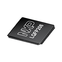
LPC2930 NXP Semiconductors, LPC2930 Datasheet - Page 13

LPC2930
Manufacturer Part Number
LPC2930
Description
The LPC2930 combine an ARM968E-S CPU core with two integrated TCM blocksoperating at frequencies of up to 125 MHz, Full-speed USB 2
Manufacturer
NXP Semiconductors
Datasheet
1.LPC2930.pdf
(98 pages)
Available stocks
Company
Part Number
Manufacturer
Quantity
Price
Company:
Part Number:
LPC2930FBD208
Manufacturer:
PHI
Quantity:
103
Company:
Part Number:
LPC2930FBD208,551
Manufacturer:
NXP Semiconductors
Quantity:
10 000
Company:
Part Number:
LPC2930FBD208551
Manufacturer:
NXP Semiconductors
Quantity:
135
Company:
Part Number:
LPC2930FET208,551
Manufacturer:
NXP Semiconductors
Quantity:
10 000
NXP Semiconductors
Table 3.
[1]
[2]
[3]
[4]
[5]
6. Functional description
LPC2930_3
Product data sheet
Pin name
P0[21]/IN2[5]/
PMAT2[3]/A17
P0[22]/IN2[6]/
PMAT2[4]/A18
V
P0[23]/IN2[7]/
PMAT2[5]/A19
P2[20]/
PCAP2[0]/D18
V
V
TDI
SS(IO)
DD(CORE)
SS(CORE)
Bidirectional pad; analog port; plain input; 3-state output; slew rate control; 5 V tolerant; TTL with hysteresis; programmable pull-up /
pull-down / repeater.
USB pad.
For LPC2930 only, these are the boot control pins for configuring the external memory bus width. Use a weak pull-up/pull-down resistor
(≈1 kΩ to 10 kΩ) to set level. See
Analog pad; Analog input/output.
Analog I/O pad.
LQFP208 pin assignment
6.1 Architectural overview
Pin
201
202
203
204
205
206
207
208
The LPC2930 consists of:
The LPC2930 configures the ARM968E-S processor in little-endian byte order. All
peripherals run at their own clock frequency to optimize the total system power
consumption. The AHB-to-APB bridge used in the subsystems contains a write-ahead
buffer one transaction deep. This implies that when the ARM968E-S issues a buffered
write action to a register located on the APB side of the bridge, it continues even though
the actual write may not yet have taken place. Completion of a second write to the same
subsystem will not be executed until the first write is finished.
•
•
•
•
•
[5]
[5]
[5]
[1]
[1]
An ARM968E-S processor with real-time emulation support.
An AMBA multilayer Advanced High-performance Bus (AHB) for interfacing to the
on-chip memory controllers.
Two DTL buses (an universal NXP interface) for interfacing to the interrupt controller
and the Power, Clock and Reset Control cluster (also called subsystem).
Three ARM Peripheral Buses (APB - a compatible super set of ARM's AMBA
advanced peripheral bus) for connection to on-chip peripherals clustered in
subsystems.
One ARM Peripheral Bus for event router and system control.
Description
Function 0
(default)
GPIO 0, pin 21
GPIO 0, pin 22
GPIO 0, pin 23
GPIO 2, pin 20
1.8 V power supply for digital core
ground for digital core
IEEE 1149.1 data in, pulled up internally
Table
…continued
11.
All information provided in this document is subject to legal disclaimers.
Rev. 03 — 16 April 2010
Function 1
ADC2 IN5
ADC2 IN6
ADC2 IN7
SPI2 SDO
ARM9 microcontroller with CAN, LIN, and USB
Function 2
PWM2 MAT3
PWM2 MAT4
PWM2 MAT5
PWM2 CAP0
LPC2930
© NXP B.V. 2010. All rights reserved.
Function 3
EXTBUS A17
EXTBUS A18
EXTBUS A19
EXTBUS D18
13 of 98


