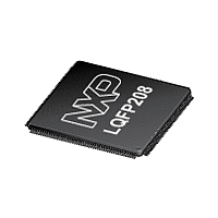
LPC2930 NXP Semiconductors, LPC2930 Datasheet - Page 76

LPC2930
Manufacturer Part Number
LPC2930
Description
The LPC2930 combine an ARM968E-S CPU core with two integrated TCM blocksoperating at frequencies of up to 125 MHz, Full-speed USB 2
Manufacturer
NXP Semiconductors
Datasheet
1.LPC2930.pdf
(98 pages)
Available stocks
Company
Part Number
Manufacturer
Quantity
Price
Company:
Part Number:
LPC2930FBD208
Manufacturer:
PHI
Quantity:
103
Company:
Part Number:
LPC2930FBD208,551
Manufacturer:
NXP Semiconductors
Quantity:
10 000
Company:
Part Number:
LPC2930FBD208551
Manufacturer:
NXP Semiconductors
Quantity:
135
Company:
Part Number:
LPC2930FET208,551
Manufacturer:
NXP Semiconductors
Quantity:
10 000
NXP Semiconductors
Table 39.
V
ground.
[1]
[2]
[3]
[4]
LPC2930_3
Product data sheet
Symbol
T
t
t
Read cycle parameters
t
t
t
t
t
t
t
t
t
Write cycle parameters
t
t
t
t
t
t
t
a(R)int
a(W)int
CSLAV
OELAV
CSLOEL
su(DQ)
h(D)
CSHOEH
BLSLBLSH
OELOEH
BLSLAV
CSHBLSH
CSLWEL
CSLBLSL
WELDV
CSLDV
WELWEH
BLSLBLSH
DD(CORE)
CLCL
All parameters are guaranteed over the virtual junction temperature range by design. Pre-testing is performed at T
temperature on wafer level. Cased products are tested at T
test conditions to cover the specified temperature and power supply voltage range.
When the byte lane select signals are used to connect the write enable input (8 bit devices), t
When the byte lane select signals are used to connect the write enable input (8 bit devices), t
For 16 and 32 bit devices.
[1]
= V
Parameter
clock cycle time
internal read access time
internal write access time
CS LOW to address valid
time
OE LOW to address valid
time
CS LOW to OE LOW time
data input /output set-up
time
data input hold time
CS HIGH to OE HIGH time
BLS LOW to BLS HIGH time
OE LOW to OE HIGH time
BLS LOW to address valid
time
CS HIGH to BLS HIGH time
CS LOW to WE LOW time
CS LOW to BLS LOW time
WE LOW to data valid time
CS LOW to data valid time
WE LOW to WE HIGH time
BLS LOW to BLS HIGH time
External static memory interface dynamic characteristics
DD(OSC_PLL)
9.5 Dynamic characteristics: external static memory
; V
DD(IO)
= 2.7 V to 3.6 V; V
Conditions
All information provided in this document is subject to legal disclaimers.
Rev. 03 — 16 April 2010
DDA(ADC3V3)
[2]
[3]
[4]
amb
Min
8
-
-
−5
−5 − WSTOEN × T
-
11
0
-
-
-
-
-
-
-
-
−0.5
-
-
= 25 °C (final testing). Both pre-testing and final testing use correlated
= 3.0 V to 3.6 V; all voltages are measured with respect to
ARM9 microcontroller with CAN, LIN, and USB
CLCL
-
-
(WSTWEN + 0.5) × T
Typ
-
−2.5
−2.5 − WSTOEN × T
0 + WSTOEN × T
16
2.5
0
(WST1 − WSTOEN +1) ×
T
(WST1 − WSTOEN +1) ×
T
0 + WSTOEN × T
0
WSTWEN × T
(WSTWEN + 0.5) × T
−0.1
(WST2 − WSTWEN +1) ×
T
(WST2 − WSTWEN +2) ×
T
CLCL
CLCL
CLCL
CLCL
CSHBLSH
CSLBLSL
= t
= −0.5 × T
CSLWEL
CLCL
CLCL
CLCL
.
LPC2930
© NXP B.V. 2010. All rights reserved.
CLCL
CLCL
amb
CLCL
CLCL
.
= 85 °C ambient
Max Unit
100
20.5 ns
24.9 ns
-
-
-
22
5
-
-
-
-
-
-
-
-
0.3
-
-
76 of 98
ns
ns
ns
ns
ns
ns
ns
ns
ns
ns
ns
ns
ns
ns
ns
ns
ns


