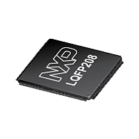
LPC2939 NXP Semiconductors, LPC2939 Datasheet - Page 28

LPC2939
Manufacturer Part Number
LPC2939
Description
The LPC2939 combine an ARM968E-S CPU core with two integrated TCM blocksoperating at frequencies of up to 125 MHz, Full-speed USB 2
Manufacturer
NXP Semiconductors
Datasheet
1.LPC2939.pdf
(99 pages)
Available stocks
Company
Part Number
Manufacturer
Quantity
Price
Company:
Part Number:
LPC2939FBD208
Manufacturer:
NXP
Quantity:
105 000
Company:
Part Number:
LPC2939FBD208,551
Manufacturer:
NXP Semiconductors
Quantity:
10 000
Company:
Part Number:
LPC2939FET208,551
Manufacturer:
NXP Semiconductors
Quantity:
10 000
NXP Semiconductors
LPC2939_3
Product data sheet
6.10.1 DMA support for peripherals
6.10 General Purpose DMA (GPDMA) controller
Usage of the idle/turn-around time (IDCY) is demonstrated In
are added between a read and a write cycle in the same external memory device.
Address pins on the device are shared with other functions. When connecting external
memories, check that the I/O pin is programmed for the correct function. Control of these
settings is handled by the SCU.
The GPDMA controller allows peripheral-to memory, memory-to-peripheral,
peripheral-to-peripheral, and memory-to-memory transactions. Each DMA stream
provides unidirectional serial DMA transfers for a single source and destination. For
example, a bidirectional port requires one stream for transmit and one for receives. The
source and destination areas can each be either a memory region or a peripheral, and
can be accessed through the same AHB master or one area by each master.
The GPDMA controls eight DMA channels with hardware prioritization. The DMA
controller interfaces to the system via two AHB bus masters, each with a full 32-bit data
bus width. DMA operations may be set up for 8-bit, 16-bit, and 32-bit data widths, and can
be either big-endian or little-endian. Incrementing or non-incrementing addressing for
source and destination are supported, as well as programmable DMA burst size. Scatter
or gather DMA is supported through the use of linked lists. This means that the source
and destination areas do not have to occupy contiguous areas of memory.
The GPDMA supports the following peripherals: SPI0/1/2 and UART0/1. The GPDMA can
access both embedded SRAM blocks (16 kB and 32 kB), both TCMs, external static
memory, and flash memory.
Fig 7.
CLK(SYS)
WE
CS
OE
D
A
WSTOEN = 2, WSTWEN = 4, WST1 = 6, WST2 = 4, IDCY = 5
Reading/writing external memory
All information provided in this document is subject to legal disclaimers.
WSTOEN
Rev. 03 — 7 April 2010
WST1
ARM9 microcontroller with CAN, LIN, and USB
IDCY
WSTWEN
Figure
WST2
7. Extra wait states
LPC2939
© NXP B.V. 2010. All rights reserved.
002aae706
28 of 99


