74LV74PW,118 NXP Semiconductors, 74LV74PW,118 Datasheet - Page 5
74LV74PW,118
Manufacturer Part Number
74LV74PW,118
Description
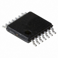
IC DUAL D FF POSEDG TRIG 14TSSOP
Manufacturer
NXP Semiconductors
Series
74LVr
Type
D-Typer
Specifications of 74LV74PW,118
Output Type
Differential
Package / Case
14-TSSOP
Function
Set(Preset) and Reset
Number Of Elements
2
Number Of Bits Per Element
1
Frequency - Clock
56MHz
Trigger Type
Positive Edge
Current - Output High, Low
12mA, 12mA
Voltage - Supply
1 V ~ 5.5 V
Operating Temperature
-40°C ~ 125°C
Mounting Type
Surface Mount
Number Of Circuits
2
Logic Family
LV
Logic Type
D-Type Edge Triggered Flip-Flop
Polarity
Inverting/Non-Inverting
Input Type
Single-Ended
Propagation Delay Time
11 ns at 3.3 V
High Level Output Current
- 12 mA
Low Level Output Current
12 mA
Supply Voltage (max)
5.5 V
Maximum Operating Temperature
+ 125 C
Mounting Style
SMD/SMT
Minimum Operating Temperature
- 40 C
Supply Voltage (min)
1 V
Delay Time - Propagation
-
Technology
CMOS
Number Of Bits
2
Number Of Elements
2
Clock-edge Trigger Type
Positive-Edge
Operating Supply Voltage (typ)
3.3V
Package Type
TSSOP
Frequency (max)
56MHz
Operating Supply Voltage (min)
1V
Operating Supply Voltage (max)
5.5V
Operating Temp Range
-40C to 125C
Operating Temperature Classification
Automotive
Mounting
Surface Mount
Pin Count
14
Lead Free Status / RoHS Status
Lead free / RoHS Compliant
Delay Time - Propagation
-
Lead Free Status / Rohs Status
Lead free / RoHS Compliant
Other names
74LV74PW-T
74LV74PW-T
935175140118
74LV74PW-T
935175140118


NXP Semiconductors
7. Limiting values
Table 5.
In accordance with the Absolute Maximum Rating System (IEC 60134). Voltages are referenced to GND (ground = 0 V).
[1]
[2]
[3]
[4]
[5]
8. Recommended operating conditions
Table 6.
Voltages are referenced to GND (ground = 0 V).
[1]
[2]
74LV74_3
Product data sheet
Symbol
V
I
I
I
I
I
T
P
Symbol
V
V
V
T
IK
OK
O
CC
GND
CC
stg
tot
CC
I
O
amb
t/ V
The input and output voltage ratings may be exceeded if the input and output current ratings are observed.
P
P
P
P
The static characteristics are guaranteed from V
V
Except for clock inputs, which have Schmitt trigger action..
tot
tot
tot
tot
CC
derates linearly with 12 mW/K above 70 C.
derates linearly with 8 mW/K above 70 C.
derates linearly with 5.5 mW/K above 60 C.
derates linearly with 4.5 mW/K above 60 C.
= 1.0 V (with input levels GND or V
Limiting values
Recommended operating conditions
Parameter
supply voltage
input voltage
output voltage
ambient temperature
input transition rise and fall rate
Parameter
supply voltage
input clamping current
output clamping current
output current
supply current
ground current
storage temperature
total power dissipation
[1]
CC
).
[2]
CC
Rev. 03 — 28 September 2007
Conditions
V
V
V
T
= 1.2 V to V
I
O
O
amb
DIP14 package
SO14 package
(T)SSOP14 package
DHVQFN14 package
< 0.5 V or V
Dual D-type flip-flop with set and reset; positive edge-trigger
< 0.5 V or V
= 0.5 V to (V
Conditions
V
V
V
V
= 40 C to +125 C
CC
CC
CC
CC
= 1.0 V to 2.0 V
= 2.0 V to 2.7 V
= 2.7 V to 3.6 V
= 3.6 V to 5.5 V
CC
= 5.5 V, but LV devices are guaranteed to function down to
I
O
> V
CC
> V
CC
+ 0.5 V)
CC
+ 0.5 V
+ 0.5 V
Min
1.0
0
0
-
-
-
-
40
Typ
3.3
-
-
+25
-
-
-
-
[1]
[1]
[2]
[3]
[4]
[5]
Min
-
-
-
-
-
-
-
-
0.5
50
65
Max
5.5
V
V
+125
500
200
100
50
CC
CC
© NXP B.V. 2007. All rights reserved.
Max
+7.0
50
-
+150
750
500
500
500
20
50
25
74LV74
Unit
V
V
V
ns/V
ns/V
ns/V
ns/V
C
Unit
V
mA
mA
mA
mA
mA
mW
mW
mW
mW
C
5 of 19
Related parts for 74LV74PW,118
Image
Part Number
Description
Manufacturer
Datasheet
Request
R

Part Number:
Description:
IC DUAL D FF POSEDG TRIG 14TSSOP
Manufacturer:
NXP Semiconductors
Datasheet:

Part Number:
Description:
NXP Semiconductors designed the LPC2420/2460 microcontroller around a 16-bit/32-bitARM7TDMI-S CPU core with real-time debug interfaces that include both JTAG andembedded trace
Manufacturer:
NXP Semiconductors
Datasheet:

Part Number:
Description:
NXP Semiconductors designed the LPC2458 microcontroller around a 16-bit/32-bitARM7TDMI-S CPU core with real-time debug interfaces that include both JTAG andembedded trace
Manufacturer:
NXP Semiconductors
Datasheet:
Part Number:
Description:
NXP Semiconductors designed the LPC2468 microcontroller around a 16-bit/32-bitARM7TDMI-S CPU core with real-time debug interfaces that include both JTAG andembedded trace
Manufacturer:
NXP Semiconductors
Datasheet:
Part Number:
Description:
NXP Semiconductors designed the LPC2470 microcontroller, powered by theARM7TDMI-S core, to be a highly integrated microcontroller for a wide range ofapplications that require advanced communications and high quality graphic displays
Manufacturer:
NXP Semiconductors
Datasheet:
Part Number:
Description:
NXP Semiconductors designed the LPC2478 microcontroller, powered by theARM7TDMI-S core, to be a highly integrated microcontroller for a wide range ofapplications that require advanced communications and high quality graphic displays
Manufacturer:
NXP Semiconductors
Datasheet:
Part Number:
Description:
The Philips Semiconductors XA (eXtended Architecture) family of 16-bit single-chip microcontrollers is powerful enough to easily handle the requirements of high performance embedded applications, yet inexpensive enough to compete in the market for hi
Manufacturer:
NXP Semiconductors
Datasheet:
Part Number:
Description:
The XA-S3 device is a member of Philips Semiconductors? XA(eXtended Architecture) family of high performance 16-bitsingle-chip microcontrollers
Manufacturer:
NXP Semiconductors
Datasheet:

Part Number:
Description:
The NXP BlueStreak LH75401/LH75411 family consists of two low-cost 16/32-bit System-on-Chip (SoC) devices
Manufacturer:
NXP Semiconductors
Datasheet:
Part Number:
Description:
The NXP LPC3130/3131 combine an 180 MHz ARM926EJ-S CPU core, high-speed USB2
Manufacturer:
NXP Semiconductors
Datasheet:
Part Number:
Description:
The NXP LPC3141 combine a 270 MHz ARM926EJ-S CPU core, High-speed USB 2
Manufacturer:
NXP Semiconductors
Part Number:
Description:
The NXP LPC3143 combine a 270 MHz ARM926EJ-S CPU core, High-speed USB 2
Manufacturer:
NXP Semiconductors

Part Number:
Description:
The NXP LPC3152 combines an 180 MHz ARM926EJ-S CPU core, High-speed USB 2
Manufacturer:
NXP Semiconductors
Part Number:
Description:
The NXP LPC3154 combines an 180 MHz ARM926EJ-S CPU core, High-speed USB 2
Manufacturer:
NXP Semiconductors