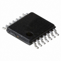
74LV74PW,118 NXP Semiconductors, 74LV74PW,118 Datasheet - Page 7

74LV74PW,118
Manufacturer Part Number
74LV74PW,118
Description
IC DUAL D FF POSEDG TRIG 14TSSOP
Manufacturer
NXP Semiconductors
Series
74LVr
Type
D-Typer
Specifications of 74LV74PW,118
Output Type
Differential
Package / Case
14-TSSOP
Function
Set(Preset) and Reset
Number Of Elements
2
Number Of Bits Per Element
1
Frequency - Clock
56MHz
Trigger Type
Positive Edge
Current - Output High, Low
12mA, 12mA
Voltage - Supply
1 V ~ 5.5 V
Operating Temperature
-40°C ~ 125°C
Mounting Type
Surface Mount
Number Of Circuits
2
Logic Family
LV
Logic Type
D-Type Edge Triggered Flip-Flop
Polarity
Inverting/Non-Inverting
Input Type
Single-Ended
Propagation Delay Time
11 ns at 3.3 V
High Level Output Current
- 12 mA
Low Level Output Current
12 mA
Supply Voltage (max)
5.5 V
Maximum Operating Temperature
+ 125 C
Mounting Style
SMD/SMT
Minimum Operating Temperature
- 40 C
Supply Voltage (min)
1 V
Delay Time - Propagation
-
Technology
CMOS
Number Of Bits
2
Number Of Elements
2
Clock-edge Trigger Type
Positive-Edge
Operating Supply Voltage (typ)
3.3V
Package Type
TSSOP
Frequency (max)
56MHz
Operating Supply Voltage (min)
1V
Operating Supply Voltage (max)
5.5V
Operating Temp Range
-40C to 125C
Operating Temperature Classification
Automotive
Mounting
Surface Mount
Pin Count
14
Lead Free Status / RoHS Status
Lead free / RoHS Compliant
Delay Time - Propagation
-
Lead Free Status / Rohs Status
Lead free / RoHS Compliant
Other names
74LV74PW-T
74LV74PW-T
935175140118
74LV74PW-T
935175140118
NXP Semiconductors
10. Dynamic characteristics
Table 8.
GND = 0 V; For test circuit see
74LV74_3
Product data sheet
Symbol Parameter
t
t
t
t
pd
W
rec
su
propagation
delay
pulse width
recovery time
set-up time
Dynamic characteristics
set or reset; see
Conditions
nCP to nQ, nQ; see
nSD to nQ, nQ; nRD to nQ, nQ;
see
clock HIGH or LOW; see
set or reset LOW; see
nD to nCP; see
Figure
V
V
V
V
V
V
V
V
V
V
V
V
V
V
V
V
V
V
V
V
V
V
V
V
V
V
CC
CC
CC
CC
CC
CC
CC
CC
CC
CC
CC
CC
CC
CC
CC
CC
CC
CC
CC
CC
CC
CC
CC
CC
CC
CC
Figure 7
= 1.2 V
= 2.0 V
= 2.7 V
= 3.3 V; C
= 3.0 V to 3.6 V
= 4.5 V to 5.5 V
= 1.2 V
= 2.0 V
= 2.7 V
= 3.3 V; C
= 3.0 V to 3.6 V
= 4.5 V to 5.5 V
= 2.0 V
= 2.7 V
= 3.0 V to 3.6 V
= 4.5 V to 5.5 V
= 1.2 V
= 2.0 V
= 2.7 V
= 3.0 V to 3.6 V
= 4.5 V to 5.5 V
= 1.2 V
= 2.0 V
= 2.7 V
= 3.0 V to 3.6 V
= 4.5 V to 5.5 V
8.
Figure 6
L
L
Figure 7
= 15 pF
= 15 pF
Rev. 03 — 28 September 2007
Figure 6
Figure 7
Dual D-type flip-flop with set and reset; positive edge-trigger
Figure
6;
[2]
[3]
[3]
[3]
[3]
[3]
[3]
[3]
[3]
[3]
[3]
Min
34
25
20
15
14
10
22
12
8
6
8
6
-
-
-
-
-
-
-
-
-
-
-
-
-
-
40 C to +85 C
Typ
9.5
70
24
18
11
13
90
31
23
14
17
12
10
10
8
7
6
5
2
1
1
1
4
3
2
1
[1]
Max
44
28
26
17
46
34
27
19
-
-
-
-
-
-
-
-
-
-
-
-
-
-
-
-
-
-
40 C to +125 C Unit
Min
41
30
24
18
15
11
26
15
10
9
7
8
-
-
-
-
-
-
-
-
-
-
-
-
-
-
© NXP B.V. 2007. All rights reserved.
74LV74
Max
56
41
33
23
58
43
34
24
-
-
-
-
-
-
-
-
-
-
-
-
-
-
-
-
-
-
ns
ns
ns
ns
ns
ns
ns
ns
ns
ns
ns
ns
ns
ns
ns
ns
ns
ns
ns
ns
ns
ns
ns
ns
ns
ns
7 of 19


