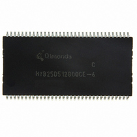
HYB25D512800CE-6 Qimonda, HYB25D512800CE-6 Datasheet - Page 28

HYB25D512800CE-6
Manufacturer Part Number
HYB25D512800CE-6
Description
IC DDR SDRAM 512MBIT 66TSOP
Manufacturer
Qimonda
Datasheet
1.HYB25D512800CE-6.pdf
(42 pages)
Specifications of HYB25D512800CE-6
Format - Memory
RAM
Memory Type
DDR SDRAM
Memory Size
512M (64M x 8)
Speed
166MHz
Interface
Parallel
Voltage - Supply
2.3 V ~ 2.7 V
Operating Temperature
0°C ~ 70°C
Package / Case
66-TSOP
Lead Free Status / RoHS Status
Lead free / RoHS Compliant
Other names
675-1008-2
Available stocks
Company
Part Number
Manufacturer
Quantity
Price
Part Number:
HYB25D512800CE-6
Manufacturer:
QIMONDA
Quantity:
20 000
1) 0 °C ≤ T
2) Under all conditions,
3) Peak to peak AC noise on
4)
5) Inputs are not recognized as valid until
6)
7) The ratio of the pull-up current to the pull-down current is specified for the same temperature and voltage, over the entire temperature and
8) Values are shown per pin.
Rev. 1.41, 2007-12
03292006-3TFJ-HNV3
Parameter
Device Supply Voltage
Output Supply Voltage
Supply Voltage,
I/O Supply Voltage
Input Reference Voltage
I/O Termination Voltage
(System)
Input High (Logic1) Voltage
Input Low (Logic0) Voltage
Input Voltage Level,
CK and CK Inputs
Input Differential Voltage,
CK and CK Inputs
VI-Matching Pull-up Current
to Pull-down Current
Input Leakage Current
Output Leakage Current
Output High Current,
Normal Strength Driver
Output Low Current,
Normal Strength Driver
V
must track variations in the DC level of
V
voltage range, for device drain to source voltage from 0.25 to 1.0 V. For a given output, it represents the maximum difference between
pull-up and pull-down drivers due to process variation.
TT
ID
is the magnitude of the difference between the input level on CK and the input level on CK.
is not applied directly to the device.
A
≤ 70 °C;
V
DD
V
DDQ
=
V
V
must be less than or equal to
DDQ
REF
= 2.5 V ± 0.2 V
Symbol
V
V
V
V
V
V
V
V
V
VI
I
I
I
I
I
OZ
OH
OL
may not exceed ± 2%
DD
DDQ
SS
REF
TT
IH.DC
IL.DC
IN.DC
ID.DC
Ratio
,
V
SSQ
V
V
V
REF
REF
TT
.
is a system supply for signal termination resistors, is expected to be set equal to
stabilizes.
Min.
2.3
2.3
0
0.49 ×
V
V
–0.3
–0.3
0.36
0.71
–2
–5
—
TBD
REF
REF
+ 0.15
– 0.04
V
Date: 2007-12-13
V
DDQ
REF.DC
V
DD
.
Electrical Characteristics and DC Operating Conditions
Typ.
2.5
2.5
0.5 ×
.
V
Values
28
REF
V
is also expected to track noise variations in
DDQ
Max.
2.7
2.7
0
0.51 ×
V
V
V
V
V
1.4
2
5
TBD
—
REF
DDQ
REF
DDQ
DDQ
+ 0.04
– 0.15
+ 0.3
+ 0.3
+ 0.6
V
DDQ
HY[B/I]25D512[40/80/16]0C[C/E/F/T](L)
512-Mbit Double-Data-Rate SDRAM
Unit Note/Test Condition
V
V
V
V
V
V
V
V
V
—
μA
μA
mA
mA
f
f
—
3)
4)
5)
5)
5)
5)6)
7)
Any input 0 V ≤
All other pins not under test
= 0 V
DQs are disabled;
0 V ≤
V
V
CK
CK
OUT
OUT
≤ 200 MHz
≤ 200 MHz
= 1.95 V
= 0.35 V
V
8)
OUT
Internet Data Sheet
V
≤
DDQ
V
TABLE 21
DDQ
2)
.
V
IN
8)
≤
V
1)
V
REF
DD
;
, and


