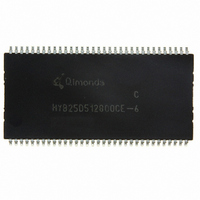
HYB25D512800CE-6 Qimonda, HYB25D512800CE-6 Datasheet - Page 32

HYB25D512800CE-6
Manufacturer Part Number
HYB25D512800CE-6
Description
IC DDR SDRAM 512MBIT 66TSOP
Manufacturer
Qimonda
Datasheet
1.HYB25D512800CE-6.pdf
(42 pages)
Specifications of HYB25D512800CE-6
Format - Memory
RAM
Memory Type
DDR SDRAM
Memory Size
512M (64M x 8)
Speed
166MHz
Interface
Parallel
Voltage - Supply
2.3 V ~ 2.7 V
Operating Temperature
0°C ~ 70°C
Package / Case
66-TSOP
Lead Free Status / RoHS Status
Lead free / RoHS Compliant
Other names
675-1008-2
Available stocks
Company
Part Number
Manufacturer
Quantity
Price
Part Number:
HYB25D512800CE-6
Manufacturer:
QIMONDA
Quantity:
20 000
1) 0 °C ≤
2) Input slew rate ≥ 1 V/ns.
3) The CK/CK input reference level (for timing reference to CK/CK) is the point at which CK and CK cross: the input reference level for signals
4) Inputs are not recognized as valid until
5) The Output timing reference level, as measured at the timing reference point indicated in AC Characteristics (note 3) is
6) For each of the terms, if not already an integer, round to the next highest integer.
7)
8) Fast slew rate ≥ 1.0 V/ns , slow slew rate ≥ 0.5 V/ns and < 1 V/ns for command/address and CK & CK slew rate > 1.0 V/ns, measured
9) These parameters guarantee device timing, but they are not necessarily tested on each device.
10) The specific requirement is that DQS be valid (HIGH,LOW, or some point on a valid transition) on or before this CK edge. A valid transition
11) The maximum limit for this parameter is not a device limit. The device operates with a greater value for this parameter, but system
Rev. 1.41, 2007-12
03292006-3TFJ-HNV3
Parameter
Write preamble setup time
Write postamble
Write recovery time
Internal write to read command
delay
Exit self-refresh to non-read
command
Exit self-refresh to read
command
other than CK/CK, is
t
voltage level, but specify when the device is no longer driving (HZ), or begins driving (LZ).
between
is defined as monotonic and meeting the input slew rate specificationsof the device. When no writes were previously in progress on the
bus, DQS will be transitioning from Hi-Z to logic LOW. If a previous write was in progress, DQS could be HIGH, LOW at this time, depending
on
performance (bus turnaround) degrades accordingly.
HZ
t
and
DQSS
T
t
.
A
LZ
V
≤ 70 °C;
IH.AC
transitions occur in the same access time windows as valid data transitions. These parameters are not referred to a specific
and
V
V
DD
V
IL.AC
REF
=
V
.
. CK/CK slew rate are ≥ 1.0 V/ns.
DDQ
= 2.5 V ± 0.2 V
Symbol
t
t
t
t
t
t
WPRES
WPST
WR
WTR
XSNR
XSRD
V
REF
stabilizes.
–5
0
0.40
15
2
75
200
DDR400
Min.
Date: 2007-12-13
32
Max.
—
0.60
—
—
—
—
–6
DDR333
Min.
0
0.40
15
1
75
200
t
CK
is equal to the actual system clock cycle time.
HY[B/I]25D512[40/80/16]0C[C/E/F/T](L)
512-Mbit Double-Data-Rate SDRAM
Max.
—
0.60
—
—
—
—
Unit
ns
t
ns
t
ns
t
CK
CK
CK
Internet Data Sheet
Note/ Test
Condition
2)3)4)5)10)
2)3)4)5)11)
2)3)4)5)
2)3)4)5)
2)3)4)5)
2)3)4)5)
V
TT
.
1)


