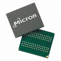
MT46H16M16LFBF-6 IT:A Micron Technology Inc, MT46H16M16LFBF-6 IT:A Datasheet - Page 6

MT46H16M16LFBF-6 IT:A
Manufacturer Part Number
MT46H16M16LFBF-6 IT:A
Description
IC DDR SDRAM 256MBIT 60VFBGA
Manufacturer
Micron Technology Inc
Type
DDR SDRAMr
Specifications of MT46H16M16LFBF-6 IT:A
Format - Memory
RAM
Memory Type
Mobile DDR SDRAM
Memory Size
256M (16Mx16)
Speed
166MHz
Interface
Parallel
Voltage - Supply
1.7 V ~ 1.95 V
Operating Temperature
-40°C ~ 85°C
Package / Case
60-VFBGA
Organization
16Mx16
Density
256Mb
Address Bus
15b
Access Time (max)
6.5/5ns
Maximum Clock Rate
166MHz
Operating Supply Voltage (typ)
1.8V
Package Type
VFBGA
Operating Temp Range
-40C to 85C
Operating Supply Voltage (max)
1.95V
Operating Supply Voltage (min)
1.7V
Supply Current
100mA
Pin Count
60
Mounting
Surface Mount
Operating Temperature Classification
Industrial
Lead Free Status / Rohs Status
Compliant
Other names
Q3368612
PDF: 09005aef82091978 / Source: 09005aef8209195b
MT46H16M16LF__2.fm - Rev. H 6/08 EN
Notes: 1. Throughout the data sheet, various figures and text refer to DQs as “DQ.” The DQ
2. Complete functionality is described throughout the document, and any page or dia-
3. Any specific requirement takes precedence over a general statement.
The 256Mb Mobile DDR SDRAM operates from a differential clock (CK and CK#); the
crossing of CK going HIGH and CK# going LOW will be referred to as the positive edge of
CK. Commands (address and control signals) are registered at every positive edge of CK.
Input data is registered on both edges of DQS, and output data is referenced to both
edges of DQS, as well as to both edges of CK.
Read and write accesses to the Mobile DDR SDRAM are burst oriented; accesses start at
a selected location and continue for a programmed number of locations in a
programmed sequence. Accesses begin with the registration of an ACTIVE command,
which is then followed by a READ or WRITE command. The address bits registered coin-
cident with the ACTIVE command are used to select the bank and row to be accessed.
The address bits registered coincident with the READ or WRITE command are used to
select the bank and the starting column location for the burst access.
The Mobile DDR SDRAM provides for programmable READ or WRITE burst lengths of 2,
4, or 8. An auto precharge function may be enabled to provide a self-timed row
precharge that is initiated at the end of the burst access.
As with standard SDR SDRAM, the pipelined, multibank architecture of Mobile DDR
SDRAM enables concurrent operation, thereby providing high effective bandwidth by
hiding row precharge and activation time.
An auto refresh mode is provided, along with a power-saving power-down mode. Deep
power-down mode is offered to achieve maximum power reduction by eliminating the
power draw of the memory array. Data will not be retained when the device enters DPD
mode.
Self refresh mode offers temperature compensation through an on-chip temperature
sensor and partial-array self refresh, which enables users to achieve additional power
savings. The temperature sensor is enabled by default, and the partial-array self refresh
can be programmed through the extended mode register.
term is to be interpreted as any and all DQ collectively, unless specifically stated oth-
erwise.
gram may have been simplified to convey a topic and may not be inclusive of all
requirements.
6
Micron Technology, Inc., reserves the right to change products or specifications without notice.
256Mb: x16, x32 Mobile DDR SDRAM
General Description
©2005 Micron Technology, Inc. All rights reserved.


