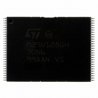
M29W128GH70N6E NUMONYX, M29W128GH70N6E Datasheet - Page 14

M29W128GH70N6E
Manufacturer Part Number
M29W128GH70N6E
Description
IC FLASH 128MBIT 70NS 56TSOP
Manufacturer
NUMONYX
Series
Axcell™r
Datasheet
1.M29W128GH70N6E.pdf
(94 pages)
Specifications of M29W128GH70N6E
Format - Memory
FLASH
Memory Type
FLASH
Memory Size
128M (16Mx8, 8Mx16)
Speed
70ns
Interface
Parallel
Voltage - Supply
2.7 V ~ 3.6 V
Operating Temperature
-40°C ~ 85°C
Package / Case
56-TSOP
Package
56TSOP
Cell Type
NOR
Density
128 Mb
Architecture
Sectored
Block Organization
Symmetrical
Typical Operating Supply Voltage
3|3.3 V
Sector Size
128KByte x 128
Timing Type
Asynchronous
Interface Type
Parallel
Lead Free Status / RoHS Status
Lead free / RoHS Compliant
Available stocks
Company
Part Number
Manufacturer
Quantity
Price
Company:
Part Number:
M29W128GH70N6E
Manufacturer:
Numonyx
Quantity:
17 280
Company:
Part Number:
M29W128GH70N6E
Manufacturer:
MICRON
Quantity:
595
Company:
Part Number:
M29W128GH70N6E
Manufacturer:
MICRON45
Quantity:
556
Part Number:
M29W128GH70N6E
Manufacturer:
ST
Quantity:
20 000
2.7
2.8
14/94
Write enable (W)
The write enable pin, W, controls the bus write operation of the memory’s command
interface.
V
The V
use an external high voltage power supply to reduce the time required for program
operations. This is achieved by bypassing the unlock cycles.
The write protect function provides a hardware method of protecting the highest or lowest
block (see
block is protected. Program and erase operations on this block are ignored while V
protect is Low.
When V
the highest or lowest block. Program and erase operations can now modify the data in this
block unless the block is protected using block protection.
When V
bypass mode (see
When V
Table 17: Program, erase times and program, erase endurance
When V
bypass program operations the memory draws I
circuits. See the description of the Unlock Bypass command in the command interface
section. The transitions from V
(see
Never raise V
memory may be left in an indeterminate state. A 0.1 µF capacitor should be connected
between the V
from the power supply. The PCB track widths must be sufficient to carry the currents
required during unlock bypass program (see I
characteristics).
The V
pull-up.
Refer to
Table 3.
PP
Figure 24: Accelerated program timing
/write protect (V
PP
PP
V
PP
PP
PP
PP
PP
V
/write protect pin provides two functions. The V
/write protect pin may be left floating or unconnected because it features an internal
Table 3
V
V
PPH
/WP
IH
/write protect is High, V
/write protect returns to V
IL
/write protect is raised to V
/write protect is raised to V
Section 1:
V
PP
PP
PP
/write protect to V
for a summary of V
/write protect pin and the V
/WP functions
Section
Highest block protected on M29W128GH.
Lowest block protected on M29W128GL.
Highest and lowest block unprotected unless a software protection is
activated (see
Unlock bypass mode. It supplies the current needed to speed up
programming.
Description). When V
6.2.6).
PP
IH
/WP)
to V
IH
PPH
Section 4: Hardware
, the memory reverts to the previous protection status of
IH
PP
PPH
PPH
PPH
from any mode except read mode, otherwise the
or V
/WP functions.
, the execution time of the command is lower (see
and from V
the memory automatically enters the unlock
IL
PP
SS
waveforms).
normal operation resumes. During unlock
/write protect is Low, V
PP1
ground pin to decouple the current surges
PP
, I
PP2
from the pin to supply the programming
Function
PPH
protection).
, I
PPH
PP3
to V
, I
function allows the memory to
IH
PP4
must be slower than t
cycles).
in
IL
Table 25: DC
, the highest or lowest
PP
VHVPP
/write


